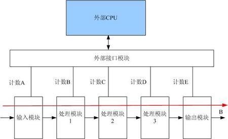
At the moment, the hottest knowledge is “big dataâ€. The core idea of ​​big data is to achieve a deeper and more intuitive understanding of the seemingly irregular behaviors of society, enterprises and individuals through scientific statistics. The measurability of the FPGA can also be used for the statistical query of the "small data" inside the FPGA to realize the exploration of the internal BUG of the FPGA. Testability design is not an unpredictable learning for FPGA design. The purpose of FPGA's testability design is to consider the issues of subsequent problem debugging, problem location, etc. at the beginning of the design. To understand the FPGA testability design, just answer a few questions, that is: (1) How is the design completed? (2) There is a problem with the design. How to locate it quickly? (3) How can I classify faults at the beginning of design and isolate problems? In general, during the debugging phase of the design, if a bug occurs, the embedded logic analyzer (chipscope/signaltap) is required to capture the signal that may be problematic. In this way, the debugging of the larger design is slower (the compile time is longer and the iteration speed is slower, but it is also a very effective means and the necessary skills of the FPGA). So what are the effective tools for the testability of large projects? (1) Statistical count. The statistical count in the FPGA design is not what "big data" is, just some "small data". For example, for the network interface, how many packets are received, how many packets are sent, how many bytes are received, and how many bytes are sent. . For a module, how many calls are received, or how many operations are initiated. For the data stream operation of the read FIFO, how many frames are read from the FIFO, and how many frames are written to the subsequent FIFO. These counts are undoubtedly resource-intensive, but taking advantage of these resources is valuable. With these counts, the design can be read by the external processor via the bus interface. So a "big data" graphic designed inside the FPGA is revealed." As can be seen from the above figure, the counts in the respective processing modules can be read out by the external CPU, and a data flow graph inside thereof is obtained. We can simplify the design as (count A->count B->count C->count D->count E). In actual use, it can be determined according to the occupied resources and the actual observation points. Assume that during the debugging process, we found that there is a sudden output without input. This is no need to go to the embedded logic analyzer to capture the signal. Through the software of the CPU, all the counts can be printed. In the case of input drivers, Assuming that the count C has changed and the count D has not changed, the processing module 3 is directly located, and the processing is problematic at this time, which is simple and effective. So that a situation can be quickly located, the input is more, but the output is less, such as the normal input code stream, but the output to the display does not lack frames and few frames, completely not smooth. Through the counting analysis, the original frame counts C and D should be the same, but the D count is much less than C, indicating that the processing module 3 performance is insufficient or the design is defective. This will locate the key points of the entire design to the processing module 3. Through the key count analysis of each module inside the FPGA, the analysis problem is located, and there is no difficulty in design. However, it requires the use of an external CPU or an FPGA embedded CPU. Everything has advantages and disadvantages. Adding more counts will increase the amount of resources used, so how to balance? A separate bit width setting is made for this analysis count, and `define REG_WIDTH N is located in the globally unified macro definition. At this time, the setting of N can be flexible, 8 bits / 16 bits / 32 bits and so on. The required logic can be flexibly added based on the remaining amount of resources in the project. After all, the values ​​of these counts provide an analysis trial. (2) Status output. If we are targeting a module like the above problem, how do we relocate the logic in the module? The key to solving this problem is the state machine, which counts the output. In the general design, the state machine is designed as the core, and the CS (current state) signal of the state machine is taken out. If there is no external output, the current The status should be IDLE. For example, in the above, we locate module 3 crashing at this time, waiting for the external signal to be no longer input. At this time, the state machine signal in module 3 is not IDLE. If it is in the state B_CS, it indicates the error of the module at this time. Appears in state B. The B jump must be activated by the signal X. Therefore, the problem of signal X can be directly located. The rest is to locate the signal X why it does not work. (3) Logic reset. Another way to divide an FPGA problem or a module problem is to have a logic reset. In the above reset (architectural design), logic reset, if the A module has a logic reset, if the design has no output (commonly known as "FPGA dead" If a module is suspected and the module is logically reset and the design works normally, then the module that needs to be located can be the module or the module that is affected by the module (the abnormal output of the module leads to the next module) Error). This article will be designed for FPGA testability, non-ASIC, by plugging in JTAG/BIST. The goal is to locate the problem and improve the testability of the FPGA by focusing on how to test the design. In addition, the logic probe is also a way to solve the test problem (special topic). The increase in testability means an increase in debugging means and an increase in debugging speed, rather than relying solely on embedded logic analyzers. The ability to achieve rapid problem location is an important manifestation of FPGA R&D capabilities, and testability design is a powerful assistant to enhance this capability. Bulkhead Lamp,Led Bulkhead Lamp,Round Bulkhead Light,Bulkhead Ceiling Light Changxing Fanya Lighting Co.,Ltd , https://www.fyledlights.com