HGST (formerly Hitachi Global Storage Technology, now a subsidiary of Western Digital (NASDAQ: WDC)) is leading the hard disk industry to the forefront of nanolithography technology and expanding its vision to semiconductor manufacturers. By creating and copying subtle parts, HGST will double the storage density of future hard disk drives (HDDs). HGST Laboratories has announced that they have successfully created large-area high-density storage media by fusing two innovative nanotechnology technologies, namely self-assembling molecular technology and nanoimprint technology, in which the width of the magnetic island is only one tenth of a billion (10 nanometers), which is only about the width of about 50 molecules side by side, or thinner than one hundred thousandth of human hair. "As a manufacturer of traditional hard drives, we can take advantage of the advances in nanotechnology today and inherit and carry forward our tradition of innovation. We are very proud," said Currie Munce, Vice President of the HGST Research Center. Emerging technologies such as India will have a huge impact on nanomanufacturing, making lattice media an economical means of increasing disk density before the end of this decade. " HGST's research results in nanolithography have overcome the challenges faced in lithography. In the semiconductor industry, lithography has always been the technology of choice when using shorter and shorter traditional light wavelengths, improved optics, masks, photosensitive materials, and smarter technologies in order to continuously realize smaller electronic components. Because UV light sources have become too complex and expensive, the development of lithography technology has been slow. HGST is becoming the leading manufacturer of nanolithography technology. The results announced today represent that HGST is solving lithography technical problems in a creative way and has surpassed the unique technical goals and stringent cost goals of the storage industry. HGST nanolithography technology achievements are emerging at a critical point in the development of the hard disk industry. Because cloud computing, social networks, and mobility are creating an ever-increasing amount of content, they must be efficiently stored, managed, and accessed. Nanolithography process At the 2013 International Society of Optical Engineering Advanced Lithography Technology Conference in San Jose, California, HGST researcher Tom Albrecht introduced HGST's nanolithography technology achievements. He introduced the patent-pending research results developed by his team in cooperation with MolecularImprints Inc. in Austin, Texas, USA. This technology can make dense magnetic islands in the 100,000 circular magnetic tracks necessary for hard disks. Self-assembling molecules use mixed polymers, called block copolymers, which consist of multiple mutually exclusive segments. These segments are covered with a thin film on the prepared surface and arranged in perfect rows. The size of the polymer segment determines the line spacing. After the formation of the polymer lattice, a chip industry process called doubling lines made tiny parts smaller, creating two separate, spaced-apart lines. These lattices are then converted into nano-imprint templates. Nano-imprinting is a precision stamping process that transfers the nano-lattice to the chip or disk substrate. Practice has proved that preparing the original surface is a key challenge so that the block copolymer forms patterns in the radial and circular paths necessary for disk storage rotation. HGST is the first to combine self-assembling molecules, double-line technology and nano-imprint technology to achieve a rectangular part with a minimum size of 10 nanometers in a circular arrangement. What was announced today provides a roadmap for how to efficiently create magnetic islands with densities much higher than current capabilities. The bit density of the HGST10 nanolattice has doubled that of current hard drives. Laboratory tests have shown that it has outstanding initial read / write and data retention capabilities. On the entire disk, it is expected that the nanoimprint process will create more than 1 trillion discrete magnetic islands. "We achieved ultra-small parts without using any traditional lithography techniques." Albrecht said, "With proper chemical processes and surface preparation, we believe that this result can be extended to smaller-sized parts." Since self-assembling molecules create repetitive patterns, researchers expect them to be best suited for making lattice magnetic media for hard drives, evenly spaced areas in computer memory, various contacts, and periodic components in other types of semiconductor chips. Although the industry is working hard to perfect the technology to meet more demanding applications, nanoimprinting and self-assembling molecules are easily introduced into fault-tolerant applications, such as hard drives or memory.
Intelligent chargers step forward to achieve intelligent, flexible and energy-efficient charging performance.
Intelligent chargers combine all the existing technology benefits and new features that assure better communications with the battery and more flexibility of use. The innovative modular design provides highly efficient charging, reliability and ease of service.
Intelligent Battery Charger,Intelligent Lipo Battery Charger,Guided Vehicle Intelligent Battery Charger,Automation Intelligent Rapid Charger Xinxiang Taihang Jiaxin Electric Tech Co., Ltd , https://www.chargers.be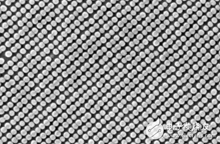
Future Disk