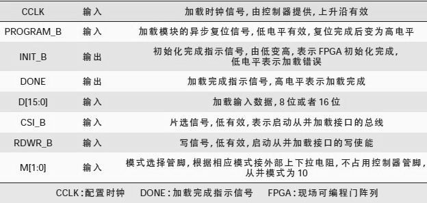
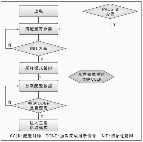
Field Programmable Gate Array (FPGA) is a semi-custom circuit in the field of application-specific integrated circuits (ASIC). It can flexibly realize the output of various interfaces or buses according to the design requirements. It has become more and more widely used in communication products at the device side. usage of. The FPGA is based on a static random access memory (SRAM) structure, and each power-up after a program loss after power-off requires a reload procedure. And with the upgrade of the FPGA scale, the loader capacity is also getting larger and larger. For example, the 6SLX150T in Xilinx's Spartan-6 series has a maximum load capacity of 4.125 MB. In communication products, the system needs to be started quickly. The FPGA load time is as short as possible, so the way it is loaded is a problem that must be properly addressed during product design. The article introduces the parallel implementation of FPGA loading mode through complex programmable logic device (CPLD), which meets the requirements of fast loading speed and low resource consumption of communication system. 1 FPGA common configuration method The configuration data of the FPGA is usually stored in the storage device in the system. After power-on, the controller reads the bit file in the memory and loads it into the FPGA. The configuration methods include JTAG, slave, slave, master and slave, and different manufacturers. The name is different, but the implementation is basically the same. (1) Boundary scan JTAG mode. The JTAG mode is commonly used in the board debugging phase. This method requires a controller, FPGA and other chip JTAG interfaces to form a daisy chain, and in this mode, other functions of the controller cannot be used. (2) From the string mode. The slave string loading method occupies less resources, mainly because there are fewer I/O interfaces connected to the FPGA, but one configuration clock can only transmit one bit of data, and the speed is relatively low. (3) Master-slave mode. The main disadvantage of this method is that the FLASH memory used must be the model specified by the FPGA manufacturer, and this FLASH capacity is not large enough to be shared with the FLASH of the controller. In this way, there will be two FLASHs on the board. Increase product costs, so the program is used less. (4) From the way. This is the FPGA loading scenario explored in the article. 2 implementation of the slave load mode Take the Xilinx Spartan-6 series FPGA as an example, and the pins related to the parallel load are shown in Table 1. Table 1 from and loading the pin name It can be seen from Table 1 that the pin resources occupied by the parallel load interface are relatively large. Even if the load data bus uses 8 bits, there are 14 pins. The CPU generally does not have so many general purpose input/output (GPIO) ports. Therefore, it is generally used in conjunction with CPLD. The loading process is shown in Figure 1. Figure 1 SPARTAN-6 slave and load process Outdoor Led Traffic Light,Solar Street Lights Outdoor,Hourglass Led Traffic Light,Lithium Battery Outdoor Solar Street Light Jiangsu Bosiwei Optoelectronics Group Co.,ltd , https://www.bswledled.com