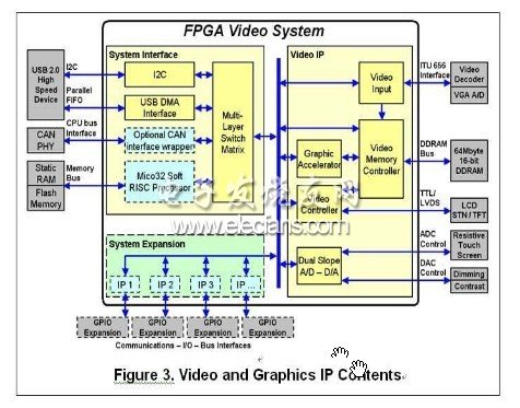
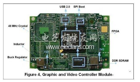
LCD monitors are really everywhere, you can see them in homes, supermarkets, gyms and cars. There is no doubt that the automotive LCD display system is the fastest growing market. The growth drivers include: declining display prices, increasing user experience, more product performance, and the accumulation of consumer products in cars. Typical graphic display systems are generally built using standard special application standard processors (ASSP) or customized special application integrated circuits (ASIC) as controllers. However, automotive graphic designers have encountered many problems when using these devices to build systems, including: shorter product life cycles, PC-based system bus interfaces, and inability to adapt to new standards and new display types. All these problems limit the possibility of reuse of the design in other applications. Figure 1: Typical graphics / video system architecture. As mentioned above, designers will encounter some obstacles when using ASSP graphics controllers in automotive design, including: 1. PC and consumer electronics products usually have a very short life cycle, but the automotive market has a long production cycle and support needs, they can not accept the changes that are forced to occur at the end of the life cycle. 2. Hard-wired ASSP or ASIC devices cannot support emerging or derived video and image standards like traditional systems. 3. The hard-wired system is also difficult to adapt to different display types, and its incompatibility is manifested in resolution, aspect ratio or display signal interface. 4. Most ASSP devices use PC bus interfaces, such as AGP, PCI and PCI Express. If a custom interface is to be built between the internal system bus and the ASSP graphics device, automotive designers will also face additional cost and complexity issues. The single chip price of ASIC is indeed quite low, but the development cost is very high. The cost of its mask can reach millions of dollars. If the design needs to be changed to support new standards or new functions, the cost of the mask must be doubled. Figure 2: Integrated on-board graphics solution. Figure 2 is an example of high integration using FPGA . This design eliminates the need for external MediaLB devices, but handles the MediaLB protocol in internal FPGA logic. The RISC processor is integrated in the form of a 32-bit IP-based soft core processor. Coupled with the graphics / video core module IP, a complete design is achieved, including support for touch screen input, LCD backlight control, memory controller, and multiple displays. The design greatly reduces the number of components in the design by integrating all major system functions into the FPGA. The use of FPGA with built-in non-volatile boot flash memory can also save more other devices. The hardware implementation of the graphics system is part of the overall project. The designer must concentrate on the function of the graphics controller in order to find the best solution for the device. For example, a customer information display (CID) may only need to display text messages and basic graphics, while a series of glass dashboards require a high-resolution smooth graphical display, because in fact it represents the use of CID to replace physical measurements and instrument measurements. Some instrument boards and navigation systems also have real-time video displays to support rear-view camera video. Such displays require a graphics controller that can support picture-in-picture and real-time video and cannot reduce the quality of other images. In addition, the flexibility required to handle multiple video streams and inputs is also a typical requirement. There are many questions that need to be answered before implementing the graphics system, because each item will affect the final hardware and IP core implementation. These issues include: 1. Is the data source a video stream, or a graphical output, or a combination of the two, or both? If it is a video stream, how many video streams are there and what is the resolution? 2. Is the final image 2D or 3D? 3. Which display technology is used, is it liquid crystal? Plasma? Or video? How many monitors and resolutions are there in total? 4. What kind of application software interface is adopted and how convenient is it to use? 5. Does the application require an extensible architecture to meet future developments and product ratings? 6. Do I need to support multiple video pages? If necessary, how much? 7. Do you need to support image scaling? What is the magnification? If zooming is required, the editing function is also required. 8. Do you need Bitblit to support high-speed graphics performance? Does the design require horizontal and vertical Bitblit options? 9. What kind of memory and bus interface does the system need? 10. Finally, do you need to support future system expansion? Figure 3: Video and graphic IP content. Figure 3 shows an example of a modular 2D graphics and video IP core. This IP represents the functions and features that current FPGA graphics IP cores can provide. This high-speed graphics core was developed specifically for embedding into FPGA systems. The memory controller can be connected to SDRAM or DDRAM, depending on the application performance and cost budget. This IP core comes with optional video input and bitblit modules that can be configured with specific performance and functions required by the design. The display controller can control a single display or dual displays using any display technology. This kind of core has a universal internal 32-bit AMBA bus, which can be easily interfaced with other internal IP cores, or connected with external logic through FPGA I / O. Figure 4: Graphics and video controller module. A complete FPGA graphics and video module is shown in Figure 4. Due to the FPGA graphics processing scheme, the physical size is small and the number of components is also very small. The size of the module is only 70x50 mm, and it can work with a single power supply of 3.3V. The on-board graphics display solution designed with FPGA devices alleviates the problems faced by ASSP and ASIC solutions. The FPGA solution makes module design and development easier, and can provide the flexibility to integrate different IP modules, depending on the cost and functional requirements of the system. FPGA realizes the high integration of the design, thereby reducing the circuit board area and reducing the number of components. The long life of the FPGA device also guarantees the long life cycle of the product. The vast majority of FPGAs are field-upgradable (some devices can even be upgraded while working), so they can easily support new standards and new functions. Standard video and graphics IP for FPGAs provide tested and proven designs that can be easily integrated into graphics solutions. Using packaged IP solutions can also accelerate system development, allowing engineers to focus on application development rather than on low-level interfaces and graphics engines. The modular graphics IP core also allows the design to include custom graphics accelerators in the video controller. In this way, the designer can make special adjustments and optimizations to the graphics processing performance of the target system. FPGAs also provide versatility to include the best bus and interface standards. This makes it possible to design the best interface for the entire system in the system architecture, rather than designing only around the graphics processor interface or bus. The design using FPGA can help the system designer to complete the control through the system interface: the entire design can be optimized to support the real-time control and display system, and the processing of the video stream will not affect the system performance. In addition, FPGA manufacturing supports density migration within the same package size, allowing more logic to be added to improve performance, or reducing logic capacity to reduce functionality, a process that does not affect PCB layout. Density migration can reduce development, production, maintenance and logistics costs. FPGA series products that have obtained AEC-Q100 Grade-2 certification are now available for shipment, and several devices with additional functions and low cost will also be available in early 2008. The latest products provide true DSP blocks and single-die non-volatile on-board flash memory, which can be used to store the contents of the internal storage area when the power is turned off. In the past, designers felt that the cost of using FPGAs in automotive systems was too high, but now FPGA costs have been reduced and functions are stronger, making the single-chip price of FPGAs extremely competitive with other graphics solutions. Using FPGA devices to build video and graphics controllers can also enable designers to improve graphics display technology in other applications. In the automotive application, by replacing the PC-related graphics controller with an FPGA device that complies with the AEC-Q100 Grade-2 standard, the product lifespan is much longer than the current ASSP solution for 2 to 3 years. Control impedance PCB Impedance Control Board,Impedance Controlled PCB,Gold Fingers PCB,Impedance Control PCB Storm Circuit Technology Ltd , https://www.stormpcb.com
Figure 1 shows a typical example of an on-board graphics / video system. The left side of the figure lists some different input signals used to drive the graphics system. This example includes a MediaLB interface, a two-wire pixel link transceiver for video, a common system interface bus, and an NTSC / PAL video encoder. Once the video and graphics information enters the system, it is processed by the general-purpose CPU, or sent directly to the graphics processor under different system architectures. In addition, most designs also include flash memory for program storage and SDRAM for storing page and video information. 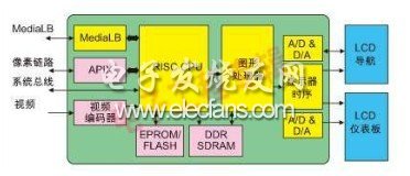
The graphics processor may be an ASSP, custom ASIC, or field programmable gate array (FPGA) device. Depending on the specific implementation, a system may contain multiple displays (as shown), and additional logic resources are required to manage various signals to support the normal operation of each display.
Multi-purpose FPGA devices with commercial intellectual property (IP) can realize almost all graphics system functions, including video controllers, RISC processors, display interfaces, bus standards, and different video input standards. All functions can be integrated on one device. 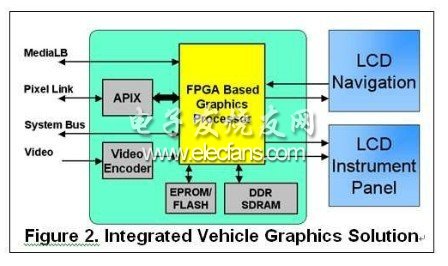
Many customers asked us what information we need for impedence control PCB.Here,there are two types for PCB manufacturer,a is single impedance ,just one trace ,two holes .and b is differential impedance,it always go with 1 pair (two trace with same width and space). For single impedance,you just tell us the trace width one which layer and what value you require .For differential impedance,trace width/space,layers and value. Our experience engineers will calculate following your instruction with Polar software.We may change trace width/space or stackup ,but please do not worry, if any changes,we will send you to approve before proceeding. Generally,the tolerance is 10%,and more accurate is 8% .All impedance boards ,we will test here and report.