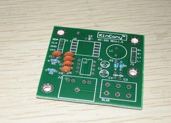
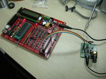
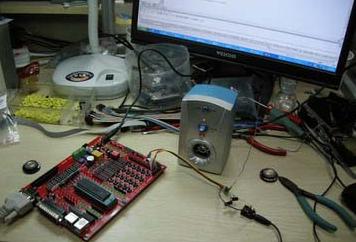
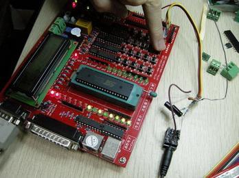
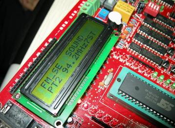
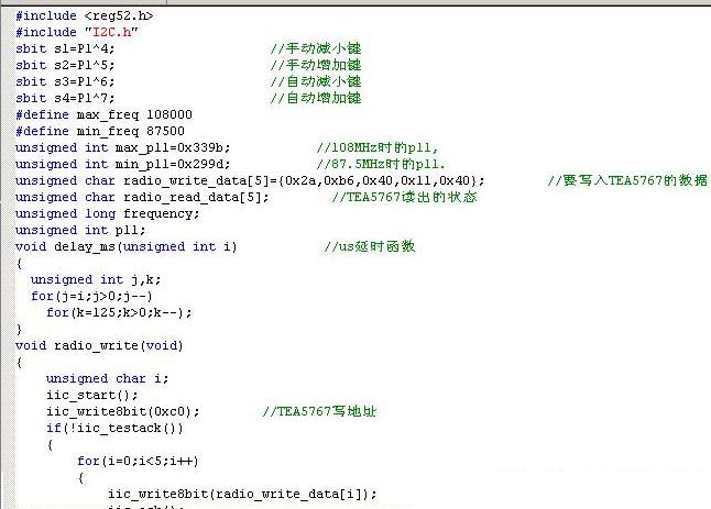
KC-201 is an FM stereo radio module, with the minimum system circuit of the single-chip computer or the single-chip microcomputer experiment board of our company, it can complete the FM broadcast reception of 88MHz-108MHz frequency. The module adopts TEA5767 / CL5767 special FM chip, the reception is stable and reliable. Onboard TDA2822 power amplifier circuit, there are left and right channel volume adjustment potentiometer. The main parameters and characteristics of the module: The following is the test process of the use of discrete components for lap welding in the development of the FM radio module: We used the 5767 radio module to connect to the experiment board through lap welding to complete the radio experiment. The commands of TDA5767 and CL5767 are fully compatible and can be replaced directly. In fact, the control of TEA5767 is not too difficult, as long as you understand TEA5767.pdf (this can be downloaded on our website), and then use C51 to control it to achieve the FM radio function. Let's talk about the programming ideas of TEA5767, I hope to help some friends who are interested in getting this chip. [page_break] KC-201 FM stereo radio module component distribution description: Module related background knowledge introduction: FM module knowledge: Software programming instructions: Table 2: Read mode IC address mode 1 1 0 0 0 0 R / W Note: 1: Read or write mode a) 0 Write to CL5767. (8): Write data Bit 6 Bit 5 Bit 4 Bit 3 Bit 2 Bit 1 Bit 0 (low order) MUTE SM PLL13 PLL12 PLL11 PLL10 PLL9 PLL8 Table 6 Description of each bit of data byte 1 symbol description 7 MUTE If MUTE = 1, left and right channels are muted; MUTE = 0, left and right channels work normally. 6 SM If SM = 1, it is in search mode; SM = 0, not in search mode. 5 to 0 PLL [13: 8] Set programmable frequency synthesizer for search and preset. Table 7 Data byte 2 format Bit 6 Bit 5 Bit 4 Bit 3 Bit 2 Bit 1 Bit 0 (low order) PLL7 PLL6 PLL5 PLL4 PLL3 PLL2 PLL1 PLL0 Table 8 Description of each bit of data byte 2 Table 9 Data byte 3 format Bit 6 Bit 5 Bit 4 Bit 3 Bit 2 Bit 1 Bit 0 (low order) SUD SSL1 SSL0 HLSI MS ML MR SWP1 Table 10 Description of each bit of data byte 3 symbol description 7 SUD SUD = 1, increase frequency search; SUD = 0, decrease frequency search. 6 and 5 SLL [1: 0] Search stop criteria: see table 1 below. 4 HLSI High / low charge current switching: HLSI = 1, high charge current; HLSI = 0, low charge current. 3 MS Stereo / Mono: MS = 1, mono; MS = 0, stereo. 2 ML Left channel mute: ML = 1, left channel mute juxtaposed stereo, ML = 0, left channel normal. 1 MR Right channel mute: MR = 1, right channel mute juxtaposed stereo, MR = 0, right channel normal. 0 SWP1 Software programmable port 1: SWP1 = 1, port 1 high level; SWP1 = 0, port 1 low level. Table 11: Search stop standard settings SSL2 Search stop criteria 0 0 Prohibited in search mode 0 1 Low: ADC output size is 5 1 0 Middle: ADC output size is 7 1 1 High: ADC output size is 10 Table 12: Format of data byte 4 Bit 6 Bit 5 Bit 4 Bit 3 Bit 2 Bit 1 Bit 0 (low order) SWP2 STBY BL XTAL SMUTE HCC SNC SI Table 13: Description of each bit of data byte 4 symbol description 7 SWP2 Software programmable port 2: SWP2 = 1, port 2 high level; SWP2 = 0, port 2 low level. 6 STBY Wait: STBY = 1, in standby mode, STBY = 0, exit standby mode. 5 BL Band system: BL = 1, Japanese FM system; BL = 0, American / European FM system. 4 XTAL If XTAL = 1, then fxtal = 32.768KHz; if XTAL = 0, then fxtal = 13MHz. 3 SMUTE Software mute: SMUTE = 1, soft mute is on; SMUTE = 0, soft mute is off. 2 HCC White level cutting: HCC = 1, high level cutting is on, HCC = 0, high level cutting is off. 1 SNC Stereo noise removal: If SNC = 1, stereo noise removal is turned on, if SNC = 0, stereo noise removal is turned off. 0 SI Search flag: SI = 1, SWPORT1 output ready signal; SI = 0, SWPORT1 is used as software programmable port 1. Table 14: Data byte 5 format Bit 6 Bit 5 Bit 4 Bit 3 Bit 2 Bit 1 Bit 0 (low order) PLLREF DTC Table 15: Each bit description of data byte 5 symbol description 7 PLLREF If PLLREF = 1, the 6.5MHz PLL reference frequency is enabled; if PLLREF = 0, the 6.5MHz PLL reference frequency is closed. 6 DTC If DTC = 1, the de-emphasis time constant is 75us; if DTC = 0, the de-emphasis time constant is 50us. 5 to 0 Not used, the status does not need to be considered. (9): Read data Bit 6 Bit 5 Bit 4 Bit 3 Bit 2 Bit 1 Bit 0 (low order) RF BLF PLL13 PLL12 PLL11 PLL10 PLL9 PLL8 Table 18: Description of each bit of data byte 1 symbol description 7 RF Ready flag: RF = 1, one channel has been found or a standard has been met; RF = 0, no channel has been found. 6 BLF Band system: BLF = 1, one system has already met; BLF = 0, no system has already met. 5 to 0 PLL [13: 8] Programmable frequency synthesizer setting result for searching and presetting. Table 19: Format of data byte 2 Bit 6 Bit 5 Bit 4 Bit 3 Bit 2 Bit 1 Bit 0 (low order) PLL7 PLL6 PLL5 PLL4 PLL3 PLL2 PLL1 PLL0 Table 20: Bit description of data byte 2 Bit 7 (high) Bit 6 Bit 5 Bit 4 Bit 3 Bit 2 Bit 1 Bit 0 (low order) STEREO IF6 IF5 IF4 IF3 IF2 IF1 IF0 Table 22: Bit description of data byte 3 symbol description 7 STEREO Stereo flag: STEREO = 1, stereo reception; STEREO = 0, mono reception. 6 to 0 IF [6: 0] IF counter result. Table 23: Data byte 4 format Bit 6 Bit 5 Bit 4 Bit 3 Bit 2 Bit 1 Bit 0 (low order) LEV3 LEV2 LEV1 LEV0 CI3 CI2 CI1 0 Table 24: Bit description of data byte 4 symbol description 7 to 4 LEV [3: 0] ADC output. 3 to 1 CI [3: 1] Chip verification number. 0 This bit is internally set to 0. Table 25: Format of data byte 5 Bit 6 Bit 5 Bit 4 Bit 3 Bit 2 Bit 1 Bit 0 (low order) 0 0 0 0 0 0 0 0 Table 26: Description of each bit of data byte 5 (10): Bus transmission schedule 27: digital level and transmission time parameter condition Minimum value Maximum unit Digital input VIH Input high 0.45VCCD V VIL Input low 0.2VCCD V Digital output Isink (L) Low level sink current 500 μA VOL Low level output voltage IOL = 500 μA 450 mV Transmission time fclk Clock input frequency I2C bus 400 kHz 3-wire 1 MHz tHIGH Clock high time I2C bus 1 μs 3-wire 300 ns tLOW Clock low time I2C bus 1 μs 3-wire 300 ns tW (write) Write pulse width 3-wire 1 μs tW (read) Read operation pulse width 3-wire 1 μs tsu (clk) Clock settling time 3-wire 300 ns th (out) Read operation data output control time 3-wire 10 ns td (out) Read operation output delay time 3-wire 100 ns tsu (write) Write operation establishment time 3-wire 100 ns th (write) Write operation control time 3-wire 100 ns
A high-quality desk lamp can help you brighten up your home office or work area so that you can finish your work and not miss a single detail. Desk lamps are also the perfect solution if you are a student and need help finishing your homework at night. Finding a light that doesn`t hurt your eyes, but illuminates your work space is important when shopping for a new desk lamp. Desk lamps also come in many shapes and sizes, so make sure you look at the dimensions of a desk lamp before purchasing based on the area you have to complete your work.
500-800 Lumen LED Desk Lamp Shenzhen Superlight Technology Co., Ltd. , https://www.superlighttech.com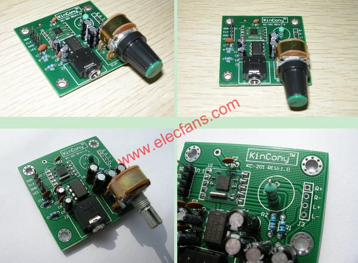
A. Use the general 102BC module package.
B. Compatible with TEA5767 and CL3767 software and hardware (software search uses IF intermediate frequency power judgment method, if the original model uses stereo judgment method, only few software changes are required).
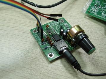
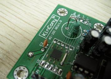
C. High sensitivity, low noise, strong interference ability, few external components, extremely simple to use, board size is 47mm * 48mm.
D. I2C serial data bus interface communication.
E. The advanced SEEK hardware search method is adopted, and the full band search only needs 4 ~ 5Sec, which greatly improves the search speed.
F. Built-in LDO adjustment, low power consumption, ultra-wide voltage range (2.7 ~ 5.5VDC).
G. Built-in noise cancellation, soft mute, bass enhancement circuit design.
H, FM and MPX stereo adopt DSP processor.
I. Simple application, low cost and high cost performance.
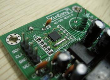
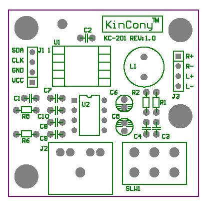
KC-201 FM stereo radio module interface description:
"J1" on the left side of the module is the IIC bus interface connected to the single chip, respectively: SDA (data), CLK (clock), GND (ground), VCC (power)
"J3" on the right side of the module is the audio output port: R + (right channel output line +), R- (right channel output line-), L + (left channel output line +), L- (left channel output line -)
The "J2" on the lower left side of the module is an external headphone jack. After the headphones are plugged in, the left and right channel audio outputs are automatically switched to the headphones. After the headphones are unplugged, the left and right channel outputs are automatically switched to the J3 output. 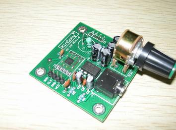
(1) First select the crystal oscillator of your hardware, which is set in the corresponding bit of the input mode, there are only two crystal options! One is 32.768KHz and the other is 13MHz. It can be controlled by XTAL of byte 4: when XTAL = 1, 32.768KH is used, and when XTAL = 0, 13MHz is used. Of course, everyone should be aware that this crystal is connected externally.
(2) Choose a good radio system, there are two modes of Japan and Europe, the frequency coverage is different.
(3) Select stereo as the output mode, and do not enable overall mute and left and right mute. This can be controlled by byte 3, please see TEA5767.pdf for details.
(4) Several other sound effect control bits can be ignored! Such as HCC, SNC. In fact, I initialized date [2] = 0x20, date [3] = 0x11, date [4] = 0x00, of course, it depends on how your hardware is connected.
(5) There are two extended output ports, which can be used for instructions and other control, but PORT1 can be used as a part-time internal status indicator, controlled by SI.
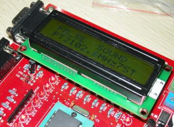
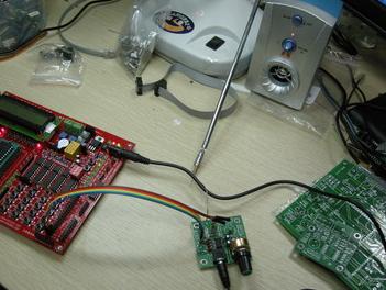
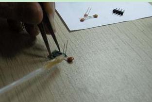
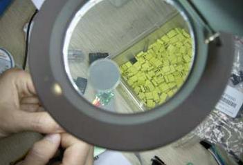
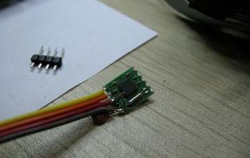
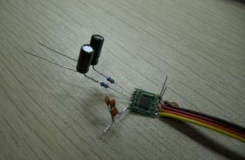
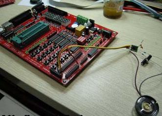
Let's share the whole process of the test below, we use the method of lap welding, because the peripheral circuit is very simple, just connect the antenna, power supply and audio output: 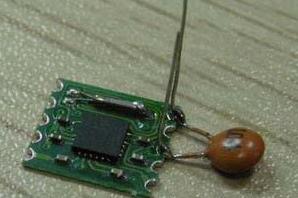
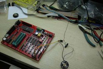
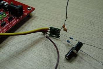
 ]
] 
CL3767 is a low-power electric tuned FM stereo radio circuit, which integrates an intermediate frequency selection and demodulation network, which can be completely free of tuning, so only a small number of small external components are required. CL3767HN can be used in different FM band environments in Europe, the United States and Japan. The product has the following characteristics:
High sensitivity (using low noise RF input amplifier)
Compatible with US / Europe (87.5 to 108 MHz) and Japan (76 to 91 MHz) FM band pre-tuned to receive Japanese TV sound to 108 MHz
High-amplifier automatic gain control (AGC) circuit
Low-cost fixed-chip FM intermediate frequency selection for LC tuning and oscillation is completed internally, and the intermediate frequency is free of three kinds of oscillation reference frequency input 32.768K, 13M, 6.5M
The phase-locked loop tuning system selects the I2C bus mode or the three-wire mode by the bus mode pin. The bus outputs 7-bit intermediate frequency count, the bus outputs 4-bit level soft mute, stereo noise cancellation (SNC), high level cutting (HCC)
Soft mute, stereo noise reduction (SNC), high-level cutting (HCC) can turn off the tuning-free stereo decoder through the bus, automatic search tuning function standby mode two software programmable ports, bus input, output line tristate mode automatic Adjustable temperature range (at VCCA, VCC (VCO) and VCCD = 5 V)
(1) I2C-bus description
The I2C bus is a bus that connects the communication between devices through two lines (serial data line and serial clock line) through two I2C buses, and identifies each device according to the address. The upper seven bits of the first byte after starting the bus is the addressing address of the slave device.
The address of the IC is C0: 1100000.
The logical structure of the I2C bus: transceiver.
The lowest bit is not used.
The maximum low level and minimum high level are limited to 0.2VCCD and 0.45VCCD respectively.
Bus mode (BUSMODE) pin must be grounded to work in I2C-bus mode. Note: The bus works at a maximum clock frequency of 400KHz. You cannot connect the IC to a bus that is working at a high clock.
(2): Data transmission data sequence: address, byte 1, byte 2, byte 3, byte 4, byte 5 (data transfer must be in order). The lowest bit of the address is "0", which means that the write operation to CL5767. The seventh bit of each byte is considered the highest bit and is transmitted as the first bit of the byte. On the falling edge of the clock, the data becomes a valid signal. The stop signal after each byte can shorten the transmission time.
A stop condition is sent before the entire transfer is complete: the reserved bytes will contain the previous information. If a word is not transmitted, the new byte will be used, but the new tuning cycle will not start. By setting the standby bit, the chip can work in a power-saving standby mode; the bus is still active. The shielded bus interface can reduce the standby current. If the bus interface is shielded, the program does not have a standby mode, the chip maintains normal operation, but has left the bus. Soft port 1 can be used as a tuning indicator output. When the channel search is not completed, soft port 1 outputs a low level. When the preset station is searched or the search is completed or the defined band is reached, the soft port 1 outputs a high level. When the maximum valid bit of the fifth byte is set to logic 1, the reference frequency of the phase-locked loop changes. The tuning system can work on the XTAL2 pin connected to the 6.5MHz crystal.
(3): Power-on reset At power-on reset, the mute position is "1" and all other positions are "0". All bits must be reset in order to initialize the integrated block.
(4): I2C-bus protocol table 1: write mode ![]()
Note: 1: S is the starting condition. ![]()
Note: 1: S is the starting condition.
2: A is the response signal. Table 3: IC address bits
b) 1 CL5767 read operation.
(5): 3-wire description 3-wire control: write / read, clock and data lines; work at a maximum clock frequency of 1MHz. Tip: Through the standby bit setting, the chip can work in a power-saving standby mode. The chip must be set to write mode in standby mode. During standby, when the chip is set to read mode, the chip will retain data. The shielded bus interface can reduce the standby current. If the bus interface is shielded, the program does not have a standby mode, and the chip maintains normal operation, but has left the clock and data lines.
(6): Data transmission data sequence: address, byte 1, byte 2, byte 3, byte 4, byte 5 (data transfer must be in order). Data can be written to the chip at the rising edge of the write / read control. Before the rising edge of the clock, the data must be a valid signal. The data signal can be changed when the clock is low, and data is written to the chip at the rising edge of the clock. After starting two bytes or each byte, if there is a new start signal, the data transmission is stopped. Data can be read from the chip on the falling edge of the write / read control. When the clock is low, the write / read control changes. The most significant bit of the first byte appears on the data side of the falling edge of the write / read control. Data is shifted on the falling edge of the clock, and data is read on the rising edge. To achieve two consecutive read or write operations, the write / read must be fixed for at least one clock cycle. When a search tuning request is sent, the chip will automatically start the search, the search direction and search stop level can be set. When a strength equal to or greater than the stop level is found, the tuning system is stopped and the ready flag is high. During the search, when a standard has been met, the tuning system stops and the standard flag is high. In this case, the ready flag is also high. Soft port 1 can be used as a tuning indicator output. When the channel search is not completed, soft port 1 outputs a low level. When the preset station is searched or the search is completed or the defined band is reached, the soft port 1 outputs a high level. When the maximum valid bit of the fifth byte is set to logic 1, the reference frequency of the phase-locked loop changes. The tuning system can work on the XTAL2 pin connected to the 6.5MHz crystal.
(7): Power-on reset At power-on reset, the mute position is "1" and all other bits are set arbitrarily. All bits must be reset in order to initialize the integrated block. 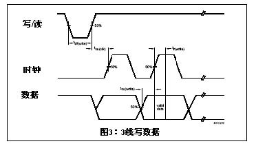
Table 4: Write Mode ![]()
Table 5 Data byte 1 format
Bit 7 (high)
Tag
Bit 7 (high) ![]()
Bit 7 (high)
Tag
SSL1
Bit 7 (high)
Tag
Bit 7 (high)
Tag 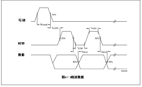
Table 16: Read Mode Table 17: Format of Data Byte 1 ![]()
Bit 7 (high)
Tag
Bit 7 (high) ![]()
Table 21: Data byte 3 format
Tag
Bit 7 (high)
Tag
Bit 7 (high) ![]()
symbol