FPGA design of BP neural network image compression algorithm multiply-accumulate unit Overview MR11 4w DIM led Spot Light is lighting with the size of the cup.
MR11 4w DIM Led Spot Light Cup points not connected with 12V and 220V transformer transformer, such as you are, then spotlights with transformer.
What you need is 12V 35W MR11 halogen lamp cup.
Lampholder two pins at different distances, MR11 4w DIM led Spot Light feet away from the common general 4mm; MR16 lamp pin pitch is generally 5.3. Some lamp base jacks are oval, light bulbs foot distance 4,5.3,6.35 apply; some lampholder socket is circular, applies only to one kind of bulb from the feet.
Low-voltage MR11 4w DIM led Spot Light constant current drive, wall lights, spot lights, buried lights, underwater lights, automotive lighting
Mingxue Optoelectronics Co.,Ltd. has apply the I S O 9 0 0 1: 2 0 0 8 international quality management system certificate, For MR11 4w DIM led Spot Light, we apply the CE, RoHS and SAA certificate for our led lighting product.
MR11 4w DIM led Spot Light Mr11 4W Dim Spot Light,Cob Mr11 4W Dim Spot Light,Bedroom Mr11 4W Dim Spot Light,Kitchen Mr11 4W Dim Spot Light Shenzhen Mingxue Optoelectronics CO.,Ltd , https://www.led-lamp-china.com
Neural Networks (Neural Networks) is short for Artificial Neural Networks (Ar-TIficial Neural Networks) and is one of the current research hotspots. After receiving a large amount of image information from the visual senses, the human brain can react quickly and reproduce the image information in the mind, which is not only related to the massive information storage capacity of the human brain, but also related to the information processing of the human brain Capabilities, including data compression capabilities. Among various neural networks, the multi-layer feedforward neural network has strong information processing capabilities. Because it uses the BP algorithm, it is also called BP neural network. Using BP neural network model can complete the compression of image data. In image compression, the processing advantages of neural networks are: massive parallelism; combining information processing and storage units; self-organizing and self-learning functions.
Compared with the traditional digital signal processor (DSP), Field Programmable Gate Array (FPGA) has more advantages in the realization of neural networks. The DSP processor adopts the order execution method during processing, and its data bit width is fixed, so the utilization rate of resources is not high, which limits the data throughput of the processor and requires a larger storage space. FPGA processing data is a hardware-based parallel processing method, that is, multiple operations can be completed in parallel in one clock cycle, which is especially suitable for the parallel characteristics of neural networks, and it can also configure the hardware structure according to design requirements, for example, according to actual needs, The bit width of data can be flexibly designed. With the rapid development of digital integrated circuit technology, the processing power of FPGA chips has been greatly improved, and it can already bear the computational volume and data throughput of neural network data compression processing. Image compression is a key technology for information transmission and storage systems. However, how to design an FPGA to achieve a given function has become the key to neural network applications.
Based on the above reasons, FPGA was selected as the implementation method of the three-layer BP neural network image compression algorithm, and a specific implementation scheme was proposed, and FPGA design and simulation verification were performed on the key units.
1 BP neural network image compression algorithm
It is common practice to call a single hidden layer feedforward network a three-layer feedforward network, which includes an input layer, a hidden layer, and an output layer. The structure of the three-layer BP neural network is shown in Figure 1. The original data node and the reconstructed data node constitute the outer layer (input layer and output layer) with a larger number of nodes, and the middle waist layer with a smaller number of nodes constitutes the compression result. The basic idea is to force the original data to pass through the narrow waist network bottleneck, and expect to obtain a more compact data representation at the bottleneck of the network to achieve the purpose of compression. In the learning process of the network, the weights of the network are adjusted through the BP training algorithm, so that the reconstructed image is as close as possible to the training image in the sense of mean square error. The trained network can be used to perform data compression tasks. The weighted value between the input layer and hidden layer of the network is equivalent to an encoder, and the weighted layer between the hidden layer and the output layer is equivalent to a decoder. The original image data input from the input terminal is processed by a neural network. The output data obtained in the hidden layer is the compression coding of the original image, and the output layer vector is the image data reconstructed after decompression. 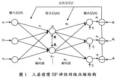
The compression ratio of BP neural network for image coding is related to the number of nodes in the input layer and hidden layer:
Compression ratio-number of input layer nodes (n) / number of hidden layer nodes (m)
Therefore, in general, different numbers of hidden layer neurons can achieve different compression ratios of the same image.
In the three-layer BP feedforward network, the input vector X = x (x1, x2, ..., xi, ..., xn) T, and the hidden layer output vector Y = y (y1, y2, ..., yi, ..., ym) T, Output layer output vector O = O (O1, O2, ..., Ok, ..., Ol) T, expected output vector d = d (d1, d2, ..., dk, ..., dl) T, the input layer to the hidden layer Weight vector V = v (v1, v2, ..., vj, ..., vm) T, where vj is the weight vector corresponding to the jth neuron of the hidden layer; the weight vector W from the hidden layer to the output layer W (w1, w2, ..., wk, ... wl) T, where wk is the weight vector corresponding to the k-th neuron of the output layer; the threshold vector of the hidden layer θ = (θ1, θ2, ..., θi, ..., θm) T; threshold vector of output layer γ = (γ1, γ2,…, γk,…, γl) T.
(1) Initialize the weights and deviations of each layer with small random numbers to ensure that the network is not saturated with large weighted inputs, and set or initialize the following parameters: minimum expected error; maximum number of cycles; correction Weight learning rate;
(2) Divide the original image into blocks of 4 × 4 or 8 × 8 size, select the pixel value of one block as a training sample and connect it to the input layer, and calculate the output of each layer: 
Among them: f (·) is the transfer function of each layer in the BP network.
(3) Calculate the error between the network output and the expected output, and determine whether it is less than the expected error, then the training is over, otherwise go to the next step, where the calculation formula of the back propagation error is: 
(4) Calculate the error transmission signal of each layer;
(5) Adjust the weights and thresholds of each layer;
(6) Check if all samples have been trained once, if yes, return to step (2), otherwise go to step (7);
(7) Check whether the network has reached the maximum number of cycles. If yes, the training ends, otherwise return to step (2).
After many trainings, finally find the best set of weights and thresholds to form a three-layer feedforward neural network for FPGA design of the algorithm. 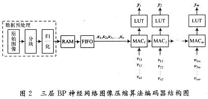
Among them, in the data preprocessing part, the original image is first divided into n × n small blocks, and normalized in units of each small block. The purpose of normalization mainly includes the following two points:
(1) The neurons of the BP network all use the Sigmoid transfer function, which can prevent the output of the neuron from being saturated due to the excessive absolute value of the net input after the transformation, and then adjust the weights to enter the flat area of ​​the error surface;
(2) The output of the Sigmoid transfer function is between -1 and +1. If the output data of the signal is not transformed, the absolute error of the output component with a large value is bound to be large, and the absolute error of the output component with a small value is small. During network training, the weight is adjusted only for the total error of the output. The result is that the output component with a small share of the total error has a relatively large error. This problem can be solved after the output is scaled.
After normalization, a matrix to be compressed consisting of column vectors is obtained with the gray value of each small block, which is stored in RAM, and then sent to the first-in first-out register FIFO (First Input FirstOutput) in units of each column; The vectors x1, x2, ..., xn are successively passed to the multiply-accumulators MAC (MulTIply-Accu-mulate) in a pipeline-line manner by the FIFO. After multiplying, accumulating and summing, they are sent to the LUT (Lookup Table) to obtain the hidden The corresponding node value of the layer, here LUT is to realize the mapping of Sigmoid function and its derivative function.
In the design of the whole circuit, the design method using a combination of IP (Intellectual Prop-erty) core and VHDL code can reload the IP soft core, which has the advantages of good versatility and easy portability, but many are charged, such as A MAC soft core with high-performance pipeline design, so based on cost considerations, use VHDL language to complete the design of the MAC module, while the RAM and FIFO modules use free reloadable IP soft core, so that the design of the entire system reaches the best cost performance. In the implementation of the compression algorithm, the multiply-accumulate unit is the common part, and also the key to the FPGA implementation of the encoder and decoder.
2.2 Multiply-accumulator MAC pipeline design and simulation
Pipeline design refers to the method of systematically dividing the combinational logic delay path, and inserting a register between each part (level) to temporarily store intermediate data. The pipeline shortens the delay path length of the combined logic circuit through which the signal passes within a clock cycle, thereby increasing the clock frequency. For a synchronous circuit, the speed refers to the frequency of the synchronous circuit clock. The faster the synchronous clock, the shorter the time interval for the circuit to process data, and the greater the amount of data processed by the circuit per unit time, that is, the greater the throughput of the circuit. In theory, the use of pipeline technology can improve the operating speed of synchronous circuits. The MAC circuit is an important part of the realization of the BP neural network, and it is also widely used in many digital signal processing fields, such as digital demodulator, digital filter and equalizer, so how to improve the efficiency and operation speed of the MAC is extremely high. value. The MAC design used in this solution takes four inputs as an example.
The four-input MAC circuit must perform four multiplication operations and two addition operations, and the last two accumulation operations. If you follow the non-pipelined design and complete the processing of the input once, the sum of these three-step delay times is required, which reduces the efficiency of a high-performance system. With the pipeline design, this delay can be avoided, and the operation of the MAC can be arranged like an assembly line. That is, through this design, it can reduce the clock cycle of the system to the slowest step in the pipeline. The operating time, not the sum of the delay times of each step, is shown in Figure 3. 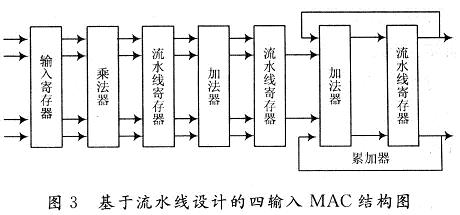
On the first clock edge, the first pair of data is stored in the input register. In the first clock cycle, the multiplier multiplies the first pair of data, and the system prepares for the input of the next pair of data. On the second clock edge, the product of the first pair of data is stored in the first pipeline register, and the second pair of data has entered the input register. In the second clock cycle, two addition operations to the first pair of data products are completed, while the multiplier completes the product operation of the second pair of data, and is ready to receive the third team of data. On the third clock edge, these data are stored in the second pipeline register, the first pipeline register, and the input register. In the third clock cycle, the first pair of data and the previous data are added and summed up, the second pair of data is added twice, the first pair of data is multiplied, and the fourth pair of data is ready to be received. On the fourth always edge, the sum in the accumulator will be updated.
In this design, the FPGA chip selected for the test simulation platform is the EP2C8 chip of the Cyclone II series of ALTERA. It uses a 90 nm manufacturing process. It has 8 256 logic cells, 36 M4K random read-only memories, and 2 digital phase locks. Ring, and 18 hard multipliers and other rich resources. The simulation tool uses the simulation software Modelsim 6.1f from the popular MentorGraphics company in the industry. When verifying a design, a common method is to apply an input excitation signal during simulation and then "read" the output signal of the design. Its main disadvantage is that it varies with the simulator. In order to overcome this shortcoming, the test method used is to write a test model generator in VHDL, called Testbench. It has the advantages of good versatility, strong flexibility, and can change the input excitation at any time, and different simulation results have been obtained. In the process of testing the MAC module, the conversion of input data is involved. As mentioned above, in this neural network, the input data is normalized and concentrated between -1 and +1, so it must be processed For conversion, the fixed-point binary representation in the form of 16-bit complement is finally used. Since overflow may occur during the summation, an overflow status signal must also be included. The simulation waveform of the input data conversion 16-bit complement is shown in Figure 4. 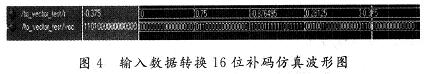
The simulation waveform of the 16-bit two's complement conversion original input real number is shown in Figure 5. 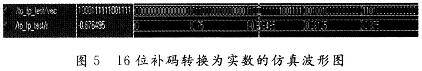
After completing the conversion of the input and output data, write a Testbench (test bench) program to conduct behavior-level simulation of the four-input MAC based on the pipeline design. The simulation waveform is shown in Figure 6. 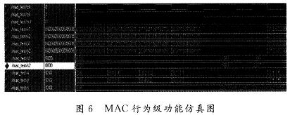
In summary, in the pipeline-based multiplication design, although registers are added after each operation, which consumes more resources, it can reduce the system delay to the time required for the slowest step, greatly improving The calculation speed of the synchronous circuit.
3 Conclusion
An image compression algorithm based on a three-layer feed-forward BP neural network is introduced, an implementation verification scheme based on FPGA is proposed, and the pipeline design of an important module MAC circuit that implements the compression network is discussed in detail. In the circuit design of the BP neural network, the linear approximation of the transfer function and its derivative function is also one of the hot topics of recent research. Although the compressed lookup table used in this paper can meet the design requirements, it still consumes a lot of resources. The research results provide a reference for the implementation of the entire compression and decompression algorithm and the related research work of the multilayer neural network.
Spotlights lights Cup MR16 and MR11 are divided into two, the former is the headlight cup, which is a small lamp cup

â—† industrial low-voltage lighting drivers
â—† Low voltage industrial lighting
â—† LED back-lighting
â—† Backlight LED Driver
â—† emergency lighting system
â—† LED driver
â—† a variety of low-voltage equipment need constant current drive


