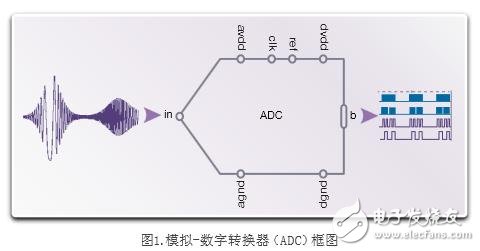
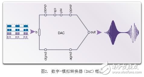
To meet demanding performance and fast-running requirements, today's systems, from communication interfaces to high-quality image, video and multimedia systems, use digital signal processing in a wide range of consumer applications. The data converter becomes the interface between the real world analog signal and the digital domain. Therefore, data converters are an important part of the complete signal processing chain, and signal processing is an integral part of every consumer electronic device. Despite the complexity of data converter design, IP vendors can provide system-on-chip (SoC) designers with data converters that can meet almost any system requirement. In addition, in order to provide data converters suitable for system-on-chip integration, well-known data converter IP vendors such as Synopsys have adopted cutting-edge circuit and architecture technologies to make them robust in demanding system-on-chip environments. These circuit and architecture techniques, which are beyond the scope of this article, eliminate the effects of substrate and power supply noise common to large system chips and are stable to process, temperature, and voltage variations. However, in order to maximize the performance of the data converter IP, the system chip designer must deal with the challenge of integrating the data converter with the system chip, avoiding the defects that endanger the performance of the entire system. The reason why data converter IP integration is considered intricate is that it requires careful manual placement and routing. However, by gaining insight into potential issues affecting performance, system-on-chip designers can have all the technical means to successfully integrate to achieve the desired performance. This article systematically introduces 12 simplified design techniques that address all common issues in system integration and help ensure successful integration of high-performance data converters in system-on-a-chip. Data converter basics Two types of data converters, analog-to-digital converters (ADCs) and digital-to-analog converters (DACs), can be selected using the architecture and configuration that best fits the performance, speed, and power requirements of system-on-chip termination applications. From a physical integration point of view, the signal interfaces of the two data converters are similar, except that the ADC converts the analog input signal into a digital output signal (Figure 1), while the DAC converts the digital input signal into an analog output signal (Figure 1 2). â–³ Analog input (in) / output (out) signals have differential transmission and single-ended transmission, which can have one, two or more channels; â–³ digital output / input (b) signal is a digital representation of the analog input / output signal; â–³ reference voltage can be input from internal reference source or external; The delta conversion clock (clk) can be driven by an internal phase-locked loop or provided externally by the chip; â–³ Provides power and ground power connections, including analog power (avdd), digital power (dvdd), analog ground (agnd), and digital ground (dgnd)
24 port PoE 10/100/1000M managed network switch/POE Switch/10/100/1000M 24 port POE
Managed POE Switch is designed for Video surveillance and network project system,etc.it provides 24x100Mbps Ethernet ports; 2x10/100/1000Mbps ports &2x1000 Base-X SFP optical fiber port as uplink ports; supports Web& CLI management,two layer network management and POE Intelligent management; supports data wire-speed and Jumbo Frame forwarding .Port based VLAN function can effectively prevent whole system from broadcast storm so that make the date transfer safer.The 16*10/100Mbps POE Switches complies with IEEE802.3 af/at standards,it simplifies wiring,avoids the troublesome of installing power socket for powered devices,such as
Features:
Application:
Gigabit Standard Managed Poe Switch Gigabit Standard Managed Poe Switch,8 Port Poe Switch,250M Poe Transmission,Giga Managed Power Dongguan Xiaoerduo Electronics Co., Ltd. , https://www.steadysmps.com