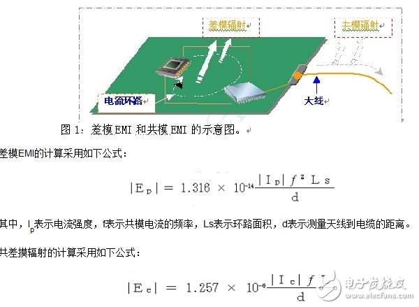
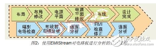
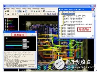
As electronic systems become more complex, EMI problems are increasing. In order to make their products meet relevant international standards, designers have to travel to and from the office and EMC labs to test, modify, and retest. It is important to find EMI problems in the product design phase. PCB layout, routing, and power layer processing have a significant impact on EMI issues across the board. This article will discuss how to use EMIStream to solve board-level EMI problems through case studies. Electromagnetic interference (EMI) is divided into two types: conducted interference and radiated interference. Conducted interference is mainly interference signals generated by electronic devices, which interfere with each other through conductive media or public power lines. Radiated interference refers to an interference signal generated by an electronic device that is spatially coupled to another circuit network or electronic device. In PCB boards, electromagnetic energy exists in two forms, differential mode EMI and common mode EMI. Differential mode EMI occurs when the current output from the device flows into a load. Common-mode EMI occurs when current flows through multiple conductive planes, such as wire sets or cables on a PCB. Figure 1 shows a schematic of differential mode EMI and common mode EMI. Where I represents the current intensity, f represents the frequency of the common mode current, L represents the length of the cable, and d represents the distance from the measuring antenna to the cable. The main method to solve EMI is to reduce the radiant energy generated by various reasons on the board. The key to controlling EMI is to reduce the ground plane resonance of the power supply and the path impedance of the circuit reflow, and correctly place the bypass and decoupling capacitors. This article uses the EMIStream tool to analyze the board EMI problem. The two main functions of the EMIStream tool are to support EMI analysis and power resonance analysis of all PCB boards. EMIStream is an application developed by NEC Corporation based on years of EMI design experience. It can be used in various PCB design processes in the design tools of companies such as Cadence, Mentor Graphics, Zuken and AlTIum to solve EMI problems before PCB manufacturing. The EMIStream software has built in 13 classic EMI inspection rules, which have been verified by the actual design results of NEC internal products in Japan. The setting value of each inspection rule is the best theoretical value that has been verified. 1. EMIStream analysis process Figure 2 shows the design flow for analyzing a board using EMIStream. EMIStream is embedded in the entire process of PCB design. Solving EMI problems during the design phase helps to reduce the number of iterations. 2. EMI check of the layout A) When the layout is complete, the Allegro data is imported directly into the EMIStream tool. EMIStream and mainstream PCB design tools from other companies such as Mentor, Zuken, and AlTIum also have interfaces to ensure complete data import. B) Set the cascading information and fill in the EMI based on the cascading information of the PCB. C) According to the design data of the circuit, correctly fill in the settings of the relevant NET frequency, crosstalk group, differential pair, and power ground signal in the circuit. D) Set the parameters of the rule, we choose to use the default parameters, and select the length check and the maximum radiation value check item to check the board. The results of the check are displayed in the form of a dialog box. The user clicks on the error prompt to view the problematic NET, and then uses the following two methods to eliminate the EMI problem: (1) adjust the layout position of the part and reduce the total length of the NET; (2) Adjust the topology of the network to reduce the intensity of common mode radiation. 3: EMI check during layout and after completion: A: After the layout and routing is completed, implement the whole board network check, and select all the key signals to be detected through the NET Parameter, such as clock, data, address line, differential pair, etc., and 13 rules can be arbitrarily selected as the benchmark for EMI check. The B:13 rule includes two rules for conducted radiation analysis, three rules for current loop analysis, two rules for power and stratigraphic analysis, four rules for signal integrity analysis, and two rules for component layout analysis. C: The results of the inspection are displayed in the form of a dialog box, which are listed one by one according to the severity of the EMI problem of the network. Open each error network, all EMI error information (error list) will be listed, some error messages will also display the modification prompt, and finally the maximum radiation value of the network and the differential mode radiation common mode radiation value will be listed; meanwhile, the network Highlights are displayed on the PCB layout and all errors are marked on the network with a red circle (Figure 3). Figure 3: The results of the check are displayed in the form of a dialog box. The error network will be highlighted on the PCB layout and all errors will be marked on the network with a red circle. For example, the first error indicates that the network does not have a complete current loop. Click on the error and the screen will zoom in and show the wrong location with a red circle. At the same time, a dialog box will pop up showing the cause of the error and suggesting several modifications. These recommendations include: (1) Modifying the path of the wire to avoid copper foil across different NETs, ​​resulting in incomplete reference planes and impedance mismatch. (2) Modify the shape of the copper foil so that the wire has a complete reference plane. The second error is the maximum radiation dB value of the network, divided into differential mode and common mode radiation values. D: Then, the found copper foil error is displayed, such as the lack of via holes at the edge of the GND copper foil, and the excessive via pitch. E: The crosstalk check helps to check if the wiring of the same layer and the walking part or the adjacent layer crosses. It is recommended to modify the traces that are too long in parallel.
Anti-Scald Electric
Kettle
Help you to boiled water in 5 minutes.
201stainless steel Electric Kettle which have passed food grand with a sleek and anti-Scald design and will compliment your kitchen counter-top
to the fullest. It is equipped with a long handle that can be used by people of
all hand sizes without straining your wrists anymore. Allow you to heat water
faster than a microwave oven and surely safer than a stovetop kettle.
Features:
· Anti-Scald Electric Kettle: Protect your hand for avoid the scald. When you touch the body, it will not
hurt you. Fill it more from the max line. We got you covered for a great and
fast Anti-Scald Electric Kettle in the market, Besides the great and nice
design, this kettle is extremely durable and will provide you endless coffee
moments with family and friends and for your morning.
· High Quality Stainless Steel Teapot: Forget all about cheaply made electric kettles and trust your coffee or tea
with our durable Stainless Steel Kettle. Keep one at the house, one at the
office and one for your camping explorations to enjoy your coffee and tees.
· Anti-Scald Handle For Easy Holding & Using: Upon
designing this electric teapot, we tried to make it extremely easy and
convenient to use. Place your hand around the handle when the water is ready,
lift the cordless kettle and pour some hot water in your cup.
· Fast Heating & Automatic Shut Off: Our Anti-Scald Electric Kettle kettle has an automatic shut off button, so as
to keep you safe when the water is ready.
· 360 Degree Rotational body with separated base: A
360-degree swivel ensures that you can pick it up from any side. Just plug it
in and place it on your kitchen counter so that everyone in your family can
pour themselves a steaming cup or water for their tea or coffee.
Application:
Make your
favourite coffee.
Prepare
comforting hot chocolate.
Cook eggs.
Anti-Scald Electric Kettle Anti-Scald Electric Kettle,Plastic Handle Kettle,Stainless Steel Kettle,Professional Electric Kettle Guangzhou Taipeng Electrical Appliances Technology CO., LTD. , https://www.taipengelectric.com