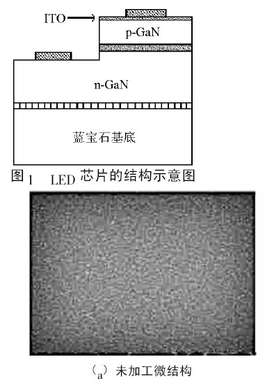
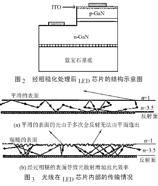
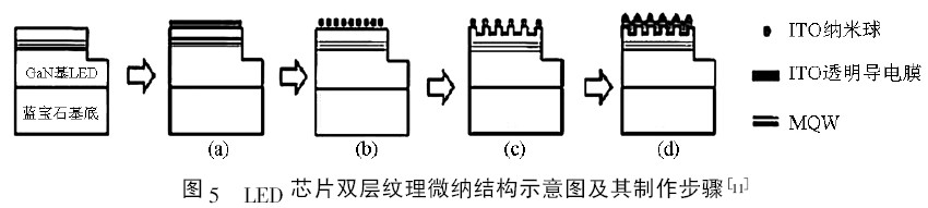
introduction Since the introduction of GaN blue LEDs in 1991, GaN-based LEDs have grown rapidly in recent years. At present, high-efficiency GaN-based LEDs have been widely used in full-color displays, solid-state lighting, and liquid crystal display backlights. LEDs have a fast growth in the LED lighting market due to their long life, low power consumption, environmental protection, impact resistance and shock resistance [1]. However, due to the total reflection caused by the difference in refractive index between the semiconductor and the air, the light extraction efficiency of the LED surface is low [2, 3], and the refractive index of the typical GaN semiconductor material is 2.5, which is obtained by the law of total reflection. It is known that the critical value of the total reflection angle of light rays from the semiconductor to the air is 24° [4], so light larger than 24° cannot escape from the semiconductor material. Therefore, total reflection greatly affects the light extraction efficiency of the LED. Therefore, how to reduce total reflection and improve the light extraction efficiency of LED has become one of the research hotspots [5]. This article mainly introduces the processing of several microstructures on the surface of LED chips or inside the chip, which can all play a role in improving the efficiency of LED light output. 1 LED surface microstructure technology Conventional GaN-based LEDs use a chemical vapor deposition (MOCVD) technique to deposit a Si-doped n-type GaN material and a Mg-doped p-type GaN material on a sapphire substrate at about 560 ° C, forming a quantum between the two materials. Well ( MQW). The p-type GaN material is further coated with an ITO film (indium tin oxide) as a transparent electrode, which functions to enhance the brightness of the electrode and to isolate electron radiation emitted from the chip, which is harmful to humans, Ultraviolet light and far infrared rays [6]. The basic structure of the LED is shown in Figure 1. Zhang Xianpeng et al. [8] of Tsinghua University adopted based on Cl2 /Ar / Inductively coupled plasma (ICP) etching of BCl3 gas produced a microstructure with a diameter of 3 μm and a period of 6 μm on the surface of p-GaN. The microstructure of the GaN-based blue LED chip is improved by 42.8%, and the LED light-emitting efficiency is increased by 38%, and the back light-emitting efficiency is improved by 10.6. %. The method of surface microstructural treatment of LED chips by Schnitzer et al. [7] of the University of California is to use a natural lithography method to roughen the light-emitting surface of the LED chip, so that the light-emitting surface of the LED chip becomes rough and uneven, roughening. The latter chip structure is shown in Figure 2. As shown in Figure 3, when light waves are transmitted to the uneven surface, more light in the semiconductor can propagate into the air due to light scattering from the rough surface. The light-emitting efficiency of the roughened LED chip can reach about 16.8%, while the light extraction efficiency of the general epoxy-encapsulated LED is very low, only about 4% [1]. The results of the roughened LED chip structure under SEM are shown in Figure 4. 2 LED chip surface double layer microstructure technology The double-layer structure on the surface of the LED chip refers to processing a thin layer on the light-emitting surface of the p-type GaN semiconductor and the upper surface of the ITO transparent conductive electrode. This double-layered micro-architecture LED chip has a light-emitting efficiency that is nearly 40% higher than that of a conventional LED chip. The fabrication method of the double-layer microstructure LED chip designed by JH Kang et al. [11] is as shown in Fig. 5. First, a 200 nm thick ITO transparent conductive film is deposited on the surface of the p-type GaN semiconductor material of the LED chip (Fig. 5). (a)), then immersed in 5% diluted hydrochloric acid for about 30s. Due to the corrosive effect of dilute hydrochloric acid on the ITO film, the 200nm ITO film will be etched into ITO nano-conductive spheres with a diameter of about 200nm (Fig. 5(b) At this time, the tiny ITO nanospheres serve as a mask structure in the subsequent etching process. After inductively coupled plasma etching (ICP), the upper surface of the etched chip p-type GaN material is formed by the protection of the nanospheres. Texture microstructure (Fig. 5(c)), and finally depositing an indium tin oxide material on the surface of the ITO nanoconducting sphere, structurally forming a double layer microstructure on the upper surface of the LED chip [10] (eg Figure 5 (d)).