Basic knowledge of interleaved ADCs
Author: ADI American engineer Jonathan Harris
In addition to the JESD204B standard definition, how much additional bandwidth does it require in many current market segments? For this problem, more complex answers always revolve around interlaced ADCs. If the ADC is interleaved, two or more ADCs with defined clock relationships are used to simultaneously sample the input signal and produce a combined output signal such that the sampling bandwidth is several times the bandwidth of a single ADC.
Interleaved ADCs are undoubtedly one of the factors driving the interface to achieve greater efficiency, providing system designers with multiple advantages. However, as converter bandwidth increases, the amount of data that needs to be processed in an FPGA or ASIC becomes very large. You must find an efficient way to handle as much data from the converter. If the sampling rate reaches the gigasample level, it will be very impractical to continue using the LVDS interface in the converter. Therefore, JESD204B is an effective way to transfer large amounts of data from a converter to an FPGA or ASIC.
Interleaved ADCs have a very broad application space. In the communications infrastructure, there is a push to increase the sampling rate of the ADC to support multi-band, multi-carrier radio in linearization technologies such as DPD (Digital Pre-Distortion) while meeting wider bandwidth requirements. . In the military and aerospace industries, higher sampling rates allow multifunction systems to be used in a variety of applications including communications, electronic surveillance and radar. ADCs with higher sampling rates are always required in industrial instrumentation applications to accurately measure higher speed signals.
First, engineers need to have some understanding of interleaved ADCs. Using m ADCs increases the effective sampling rate by a factor of m. For the sake of brevity and ease of understanding, this article focuses on the case of two ADCs. In this case, if each of the two ADCs has a sampling rate of fS and is interleaved, the final sampling rate is 2fS. These two ADCs must have a clock phase relationship for proper interleaving. The clock phase relationship is given by Equation 1, where: n is a particular ADC and m is the total number of ADCs.
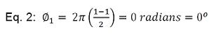
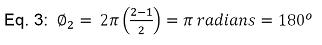
For example, both ADCs sample at 250 MSPS and are interleaved, so the sampling rate is 500 MSPS. At this point, Equation 1 can be used to derive the clock phase relationship of the two ADCs, such as Equation 2 and Equation 3.
Radian =
Note that if the clock phase relationship is known, the sample structure can be checked. Figure 1 graphically illustrates the clock phase relationship and the sample structure of two 250 MSPS interleaved ADCs.
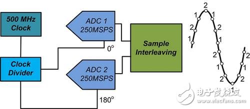
Figure 1 Two Interleaved 250MSPS ADCs – Basic Schematic
Note the 180° clock phase relationship and how the samples are interleaved. The input waveform can also be sampled by two ADCs. At this point, interleaving can be achieved with a 500MHz clock input divided by two. The divider is responsible for sending the required clock phase to each ADC.
This concept can also be expressed in another way, as shown in Figure 2.
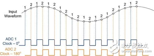
Figure 2 Two Interleaved ADCs – Clock and Sampling
By combining the two 250MSPS ADCs in an interleaved manner, the sampling rate can be increased to 500MSPS. This allows the Nyquist zone of the converter to be extended from 125MHz to 250MHz, thereby doubling the available bandwidth during operation. The increase in working bandwidth can bring many benefits. The radio system can increase the number of bands it supports; the radar system can increase the spatial resolution; and the measurement device can have a higher analog input bandwidth.
ZGAR Glo-X Prefilled Cartridge
Zgar International (M) SDN BHD , https://www.oemvape-pen.com