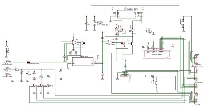
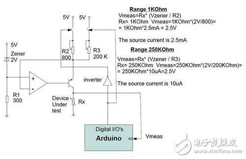
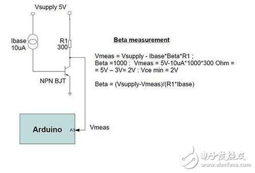
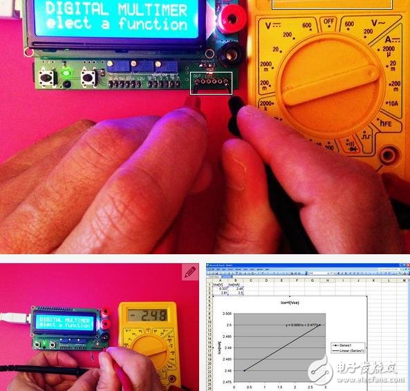
- This article is selected from the "Test and Measurement Special Issue" in May. • Separate – Measurement data can be viewed in the form of a character or graphic LCD display module. • Connection - You can use the Arduino IDE serial display to connect to your PC for reading. · Combination - Data can be viewed on both devices. The second mode does not require an LCD display module, so the price will be slightly lower. The Arduino multimeter designed for this project should have the following functions: ·Voltage meter with 3 ranges: 0-10V, 0-30V, 0-100V · One-meter ammeter: 0-500mA · ohmmeter with 2 ranges: 0-1KΩ, 0-250KΩ ·Diode, LED connectivity test ·LED functional test ·Measurement of BETA value of NPN bipolar junction transistor 1 Warning: High voltage danger! First of all, I have to release this warning, because some of our operating voltages are higher than the safe voltage value, we should always put safety in our hearts. In addition, it should be reminded that when the multimeter is connected to a computer, the computer and the device should be shared. 2 circuit design, this is the overall circuit diagram. Because the overall circuit diagram looks a bit complicated, I will divide it into sub-modules for explanation. 3 A simplified diagram of the voltmeter. The three ranges can be selected via the buttons on the Arduino board. When making a voltage measurement, only one switch is closed. 4 A simplified diagram of the ammeter. The measured current flows through the 1Ω resistor to ground, and its output is amplified and connected to the Ar1 interface of the Arduino. The gain of the amplifier is 10. For overcurrent protection, I configured a 500mA reset PTC. A simplified diagram of a 5 ohm meter. A reference voltage is generated by the Zener diode relative to the positive voltage source, the voltage being applied to a current converter consisting of a PMOS transistor and an operational amplifier connected to the source of the transistor. At this time, the voltage on the Zener diode is equal to the voltage across the resistor. 6 Arduino board control, both switches are closed, both resistors have current flowing. Therefore the current has two possible values: 10uA and 2.5mA. These currents can be precisely modulated. The generated current then flows through the device under test (resistors, diodes, LEDs...) and the voltage drop is detected at the A2 port of the Arduino. If the resistance is in the range of 100Ω. At this point, a reference current of 2.5 mA flows through the resistor and the resulting voltage is applied to the ADC input of the Atmega chip. We want to measure between 0-1000 Ω. The measured voltage also varies between 0 and 2.5V. Vce (Vds) has a voltage range of 0.5V to 3V. These two voltages directly affect the collector-emitter/source-drain current, which ultimately leads to a decrease in accuracy. This phenomenon can be well understood by this figure: the transmission characteristics of NPN bipolar junction transistors. This effect can be corrected by software, but if it is non-linear, calibration can be very difficult. ----------------------- More test and measurement technology essays can be downloaded from the special issue page - "Test and Measurement Special" 7 How to measure the beta value: The aforementioned current can flow through different devices: resistors, diodes, LEDs, Schottky diodes..., and the resulting voltage drop is related to the corresponding device. This voltage value can provide information about the corresponding device, such as the voltage drop of the device and the corresponding device: diode -0.4V-0.8V; Schottky diode -0.1V-0.5V, LED (different colors are not the same) -1.1V -3.5V. The current used at this time is 10 uA. And if you use 2.5mA, then the LED will start to emit light and you can measure the functionality of the LED. The beta value is also measured using 10uA and the measured value can be read on the screen. 8 required bill of materials. 9 PCB design documents. 10 After the PCB file is completed, it will be processed by the foundry. I waited for two weeks to get the finished product. 11 Installation and welding, this is not a big problem, careful care is the key. 12 Some explanations on the PCB. 13 Install the components. 14 To configure the Arduino, you need to configure both the mode selection and the multimeter software. The relevant configuration files can be found at http://Digital-multimeter-shield-for-Arduino/. 15 Then you need to calibrate. Find a standard multimeter and calibrate it. 16 Measure the battery voltage and you can see the selected range and voltage value information. 17 Calibrate the ohmmeter. 18 Once you are done, you are ready to test. -----------------------
The 8 layer PCB is a circuit board with 8 layers that are stacked firmly together with predefined and dependable mutual connections between the layers. Structure of eight layer PCB is more complicated. Nowadays, PCBs frequently have 8 to 12 layers or more, and electronics engineers know that designing for so many layers requires a well-configured layer stack.
8-layer Printed Circuit Boards are usually installed in compact equipment with strict spacing requirements, such as notebook computer motherboard, communication backplane, wearable watches, etc. Because of its complexity and high manufacturing costs, your 8-layer PCB Manufacturing should be made by reliable and experienced manufacturers. Jinghongyi PCB has been specially targeting high-end PCB manufacturing and assembly services for 8 years, providing high-quality products and services for various customers. Our advanced production line and fast response team will keep you comfortable and reassured, without any trouble, you can rest assured to place the order with us.
Standard stackup of 8 layer PCB looks as follows
8 Layer PCB Stack up
8 Layer PCB stackup
A typical 8 Layer PCB Stackup
0.062[8 layer PCB stackup
0.093[ 8-Layer PCB Stackup
8 LAYER 1.6 MM STANDARD STACKUP AND THICKNESS
JHYPCB is one of the leading 8 layer PCB manufacturers. For more information, pls send email to us.
8 Layer PCB PCB Circuit Board,8 Layer PCB,Custom multilayer pcb,Custom 8 Layer PCB JingHongYi PCB (HK) Co., Limited , https://www.pcbjhy.com
Design requirements: This project can use Arduino Uno or Duemilanove board, with three design modes: 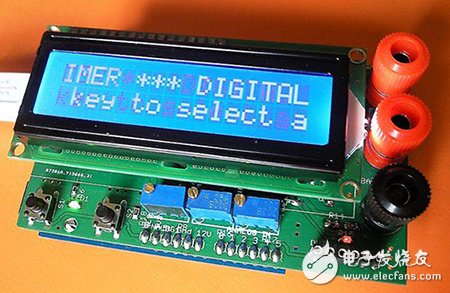


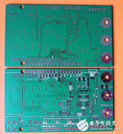
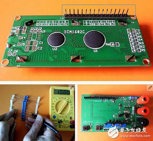


8 Layer PCB - Stackup & Cost & Prototype manufacture
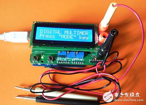
What is 8 layer PCB?

Typical 8-layer PCB stack up methods and guidelines
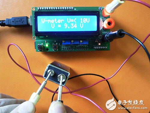
Eight-layer PCB can be used to add two additional layers, or two planes can be added to improve EMC performance. Most eight-layer circuit boards are superimposed to improve EMC performance, rather than adding additional wiring layers. Compared with 6-layer circuit boards, the cost increase percentage of 8-layer PCB is less than that of 4-layer PCB to 6-layer PCB. Therefore, in order to improve EMC performance, the cost increase is reasonable. Therefore, most 8-layer boards consist of four wiring layers and four planes.


In short, 8 layer PCB are usually used to improve the EMC performance of circuit boards, rather than increasing the number of layers.
No matter how you decide on the stack layer, it is not recommended to use an 8-layer PCB Board with six wiring layers. If you need six routing layers, you should use a 10 Layer PCB board. Therefore, the 8-layer board can be regarded as the six-layer board with the best EMC performance.
Basic Layer of Eight-Layer Circuit Board with Excellent EMC Performance

All signal layers are adjacent to the plane, and all layers are tightly coupled. High-speed signals are buried between planes, so planes provide shielding to reduce the transmission of these signals. In addition, the circuit board uses multiple grounding layers to reduce the grounding impedance.
Other forms of 8-layer PCB stackup


So far, we have also clarified the cost and price differences between 6-layer PCB, 8-layer PCB and 10-layer PCB.
8 Layer PCB thickness

8 Layer Stackup - 1.6mm thickness
layer order
layer name
material type
material description
dielectric constant
thickness
copper weight
1
top
copper
signal
0.035mm
1 oz
2116
prepreg
4.5
0.12mm
2
inner 1
copper
plane
1 oz
core
4.6
0.3mm
3
inner 2
copper
plane
1 oz
7630
prepreg
4.7
0.2mm
4
inner 3
copper
plane
1 oz
core
4.6
0.3mm
5
inner 4
copper
plane
1 oz
7630
prepreg
4.7
0.2mm
6
inner 5
copper
plane
1 oz
core
4.6
0.3mm
7
inner 5
copper
plane
1 oz
2116
prepreg
4.5
0.12mm
8
bottom
copper
signal
0.035mm
1 oz
Final board thickness: 1.6mm±0.13mm
8-Layer Prototype PCB Manufacturing Service
The 8-layer prototype FR-4 PCB is an 8-layer circuit board, which is firmly stacked together with predefined and reliable interconnection between layers. The 8-layer FR-4 PCB has more complex structure. JHYPCB is a large enterprise located in Shenzhen, China, which can manufacture 8-layer prototype PCB.
JHYPCB can provide you with multi-layer PCB board in accordance with RoHS standard. With laminated material, it can match high temperature in assembly process. Importantly, some lead-free assembly processes will require laminated substrates to withstand temperatures exceeding 260 degrees Celsius or 500 degrees Fahrenheit over a longer period of time. To solve this problem, we have high temperature laminates in stock, so that our customers can meet the higher temperature cycle requirements of some lead-free assembly applications.
