Professor Wu Mengqi from the Department of Electrical Engineering at Tsinghua University in Taiwan has developed high-frequency light-emitting diodes ( LEDs ) using nitride material properties, which can be applied to visible light communication and high-resolution displays in the future. The research team of Professor Xu Shuohong from Tsinghua University in Taiwan also used nitride materials to develop innovative semiconductor component technologies that provide high power and high efficiency wireless power transmission. Professor Wu Mengqi from the Department of Electrical Engineering at Tsinghua University in Taiwan has developed high-frequency light-emitting diodes (LEDs) using nitride material properties, which can be applied to visible light communication and high-resolution displays in the future. The research team of Professor Xu Shuohong from Tsinghua University in Taiwan also used nitride materials to develop innovative semiconductor component technologies that provide high power and high efficiency wireless power transmission. Both innovations have been internationally recognized and have been published in the leading international journal of electronic components, IEEE Electron Device Letters, and have been thoroughly reported by the renowned semiconductor industry technology magazine SemiconductorToday. The “High-Frequency Modulated Light-Emitting Diode (LED)†technology developed by Professor Wu Mengqi’s research team is based on the characteristics of nitride materials and uses Atomic Layer Deposition (ALD) to control the precision of the film to about one atomic layer. Deposition thickness, high uniformity and high depth of the nanometer grade. At present, Professor Wu Mengqi's laboratory has developed a transparent conductive film capable of growing high coverage, high transmittance and low resistivity, and is applied to photoelectric components such as light-emitting diodes, photodetectors and transparent transistors. The brightness and bandwidth of the design components are beyond the traditional limits and are leading international standards. Future applications using "high-frequency modulated light-emitting diode (LED)" technology, including optical communications, plant lighting and high-resolution displays. Optical communication is a new type of data transmission technology. It can not only use led lighting , but also use light source to transmit signals to personal computers, mobile phones or TVs. It can be used as indoor high-speed wireless Internet access, and can also be applied to vehicle light security systems. Use, to help car owners understand the state of the surrounding vehicles, timely response. Professor Wu Mengqi has made great achievements in the field of long-term cultivation of photovoltaic components. His other research paper “3D colloidal photonic crystals as the bottom mirrors to enhance the light-receiving efficiency of light-emitting diodes†was also awarded the Science and Technology Paper Award in May this year. As mobile communications become more and more important in life, wireless power supply technology has become the hottest technology application, and people can easily charge their mobile phones by simply placing them on a charging sensor. At present, the most advanced wireless charging technology is also studied in the direction of direct long-distance transmission of power. In order to improve the application range and provide high-power and high-efficiency power transmission, Professor Xu Shuohong's research team has developed high-crash voltage and low leakage by utilizing the high electron mobility of large-gap-level large electric field in gallium nitride (GaN). The current silicon substrate GaN transistor" breaks through the shortcomings of the traditional single structure electrode, which is easy to have leakage current and dielectric breakdown. The design concept of the hybrid electrode structure is proposed, the electric field distribution in the transistor is changed, and the leakage current of the component is greatly reduced. Effectively increase the breakdown voltage and overcome the shortcomings and limitations of traditional power components. This component can be grown on a large area of ​​silicon wafers, resulting in lower cost, and has the potential to be combined with silicon-based oxygen semiconductor transistors (MOSFETs), breaking through the problems of MOSFETs in power and high-speed applications, bringing great business opportunities. . Professor Xu Shuohong's research can greatly improve the efficiency of wireless power supply technology, and can be applied to the power supply of high-efficiency cloud servers, which is a key technology to improve the performance of next-generation power transmission systems. The research results of Professor Xu Shuohong's team have been internationally recognized. The relevant research has published many papers in the top journals in the field of international electronic components, and this technology has been successfully transferred to well-known semiconductor manufacturers at home and abroad, and won a considerable amount of royalties for the school. .
The 8 layer PCB is a circuit board with 8 layers that are stacked firmly together with predefined and dependable mutual connections between the layers. Structure of eight layer PCB is more complicated. Nowadays, PCBs frequently have 8 to 12 layers or more, and electronics engineers know that designing for so many layers requires a well-configured layer stack.
8-layer Printed Circuit Boards are usually installed in compact equipment with strict spacing requirements, such as notebook computer motherboard, communication backplane, wearable watches, etc. Because of its complexity and high manufacturing costs, your 8-layer PCB Manufacturing should be made by reliable and experienced manufacturers. Jinghongyi PCB has been specially targeting high-end PCB manufacturing and assembly services for 8 years, providing high-quality products and services for various customers. Our advanced production line and fast response team will keep you comfortable and reassured, without any trouble, you can rest assured to place the order with us.
8 Layer PCB Stack up
8 Layer PCB stackup
A typical 8 Layer PCB Stackup
0.062[8 layer PCB stackup
0.093[ 8-Layer PCB Stackup
8 LAYER 1.6 MM STANDARD STACKUP AND THICKNESS
JHY PPCB is one of the leading 8 layer PCB manufacturers. For more information, pls send email to us.
8 Layer PCB PCB Circuit Board,8 Layer PCB,Custom multilayer pcb,Custom 8 Layer PCB JingHongYi PCB (HK) Co., Limited , https://www.pcbjhy.com
8 Layer PCB - Stackup & Cost & Prototype manufacture
What is 8 layer PCB?
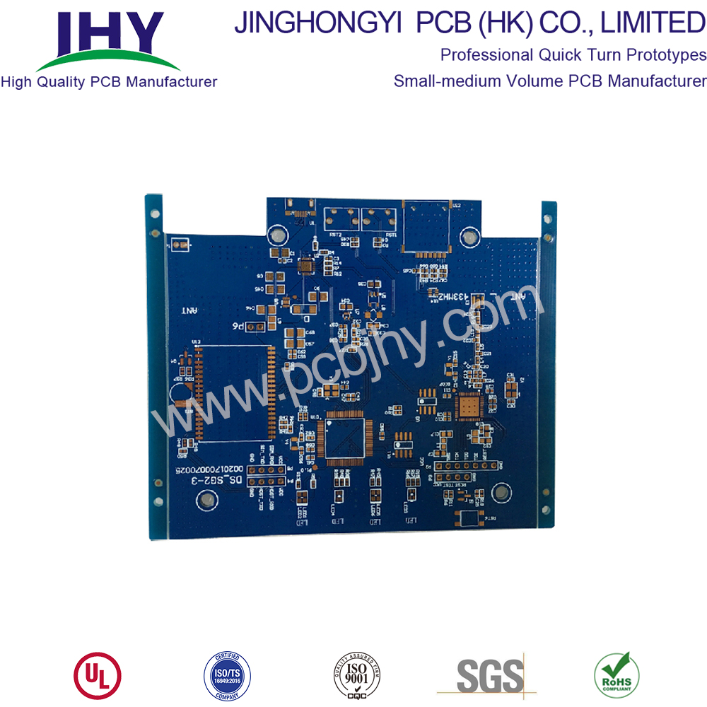
Typical 8-layer PCB stack up methods and guidelines
Standard stackup of 8 layer PCB looks as follows
Eight-layer PCB can be used to add two additional layers, or two planes can be added to improve EMC performance. Most eight-layer circuit boards are superimposed to improve EMC performance, rather than adding additional wiring layers. Compared with 6-layer circuit boards, the cost increase percentage of 8-layer PCB is less than that of 4-layer PCB to 6-layer PCB. Therefore, in order to improve EMC performance, the cost increase is reasonable. Therefore, most 8-layer boards consist of four wiring layers and four planes.
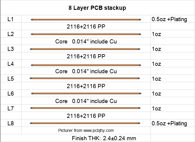
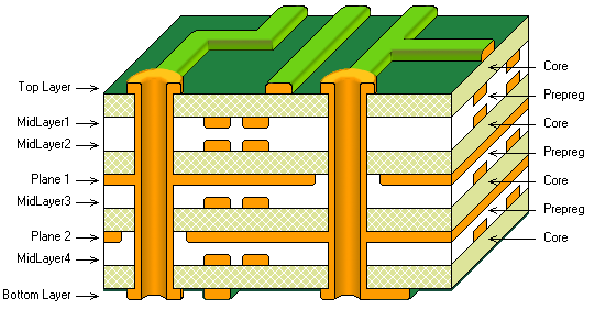
In short, 8 layer PCB are usually used to improve the EMC performance of circuit boards, rather than increasing the number of layers.
No matter how you decide on the stack layer, it is not recommended to use an 8-layer PCB Board with six wiring layers. If you need six routing layers, you should use a 10 Layer PCB board. Therefore, the 8-layer board can be regarded as the six-layer board with the best EMC performance.
Basic Layer of Eight-Layer Circuit Board with Excellent EMC Performance
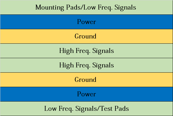
All signal layers are adjacent to the plane, and all layers are tightly coupled. High-speed signals are buried between planes, so planes provide shielding to reduce the transmission of these signals. In addition, the circuit board uses multiple grounding layers to reduce the grounding impedance.
Other forms of 8-layer PCB stackup
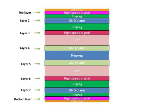
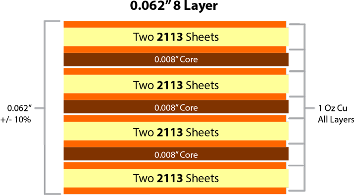
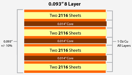
So far, we have also clarified the cost and price differences between 6-layer PCB, 8-layer PCB and 10-layer PCB.
8 Layer PCB thickness
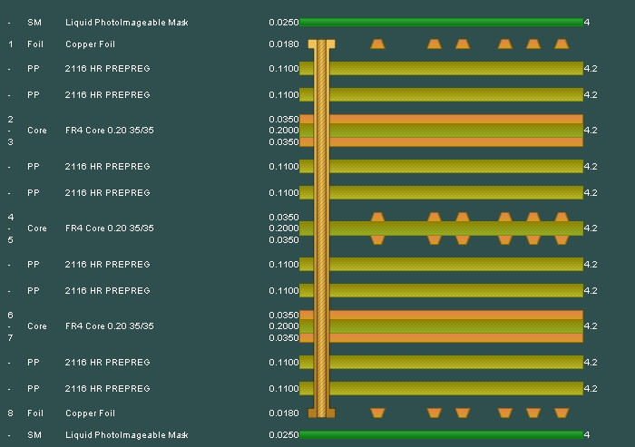
8 Layer Stackup - 1.6mm thickness
layer order
layer name
material type
material description
dielectric constant
thickness
copper weight
1
top
copper
signal
0.035mm
1 oz
2116
prepreg
4.5
0.12mm
2
inner 1
copper
plane
1 oz
core
4.6
0.3mm
3
inner 2
copper
plane
1 oz
7630
prepreg
4.7
0.2mm
4
inner 3
copper
plane
1 oz
core
4.6
0.3mm
5
inner 4
copper
plane
1 oz
7630
prepreg
4.7
0.2mm
6
inner 5
copper
plane
1 oz
core
4.6
0.3mm
7
inner 5
copper
plane
1 oz
2116
prepreg
4.5
0.12mm
8
bottom
copper
signal
0.035mm
1 oz
Final board thickness: 1.6mm±0.13mm
8-Layer Prototype PCB Manufacturing Service
The 8-layer prototype FR-4 PCB is an 8-layer circuit board, which is firmly stacked together with predefined and reliable interconnection between layers. The 8-layer FR-4 PCB has more complex structure. Jinghongyi PCB is a large enterprise located in Shenzhen, China, which can manufacture 8-layer prototype PCB.
Jinghongyi PCB can provide you with multi-layer PCB board in accordance with RoHS standard. With laminated material, it can match high temperature in assembly process. Importantly, some lead-free assembly processes will require laminated substrates to withstand temperatures exceeding 260 degrees Celsius or 500 degrees Fahrenheit over a longer period of time. To solve this problem, we have high temperature laminates in stock, so that our customers can meet the higher temperature cycle requirements of some lead-free assembly applications.
