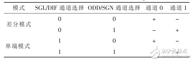
Table 1 ADC0832 Multiplexing Mode Figure 2 ADC0832 and AT89S52 Interface Circuit Telecom Battery Cabinet,Equipment Rack,Outdoor Electrical,Battery Cabinet Guangdong Yuqiu Intelligent Technology Co.,Ltd , https://www.cntcetltd.com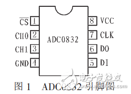
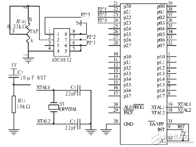
Adc0832 and at89s52 interface circuit and vacuum data acquisition
Vacuum systems are extensively applied across various industries such as electric power, petrochemicals, medical and pharmaceutical sectors, plastics, environmental protection, and medical equipment. As the application of vacuum technology continues to expand and deepen, the demands on its performance are also increasing. For example, in diamond coating devices, where the deposition process can last for several tens of hours, the stability of the vacuum within the chamber significantly affects the quality of the deposited film. Therefore, maintaining a stable vacuum has become a critical technical challenge. In the vacuum pumping process involving centrifugal pumps, the vacuum level at the pump’s inlet serves as an essential parameter for determining start/stop operations and fault diagnosis. To achieve this, the analog signal from a pressure sensor must be effectively converted into a digital format through A/D conversion before being processed by the MCU and transmitted to a PC for waveform display and analysis. The author proposes using a combination of ADC0832 and a pressure sensor (PTB710), with the AT89S52 microcontroller managing the conversion process through clock pulse control.
**1. A/D Conversion Circuit**
**1.1 ADC0832 Chip Pin Description**
Figure 1 shows the pin layout of the ADC0832. The CS pin is the chip select terminal, which is active low. CH0 and CH1 are the two analog input channels. DI is used for selecting the input channel, while DO is the serial output for the digital conversion result. CLK is the serial clock input, VCC (or REF) provides the positive supply and reference voltage, and GND is the ground connection.