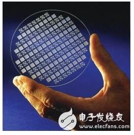
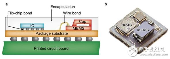
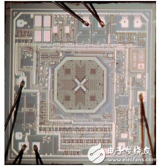
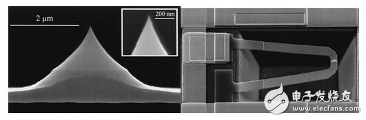
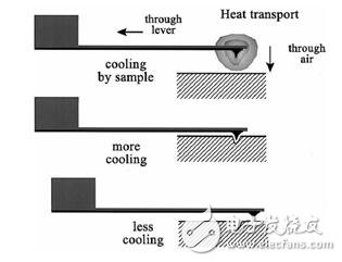
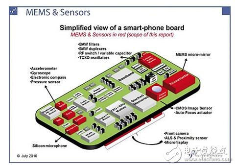
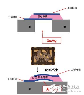
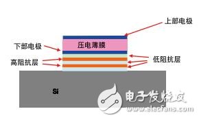
Although most people are still familiar with MEMS (Microelectromechanical systems, MEMS / micro-mechanical / micro-system), in fact, MEMS in our production, and even life has long been ubiquitous, smart phones, fitness bracelets, printers, Automotive, drones, and VR/AR headsets, some early and almost all recent electronics have applied MEMS devices. MEMS is a comprehensive discipline, interdisciplinary phenomenon and its obvious, mainly related to micro-machining technology, mechanical / solid acoustic wave theory, heat flow theory, electronics, biology and so on. MEMS devices feature lengths from 1 mm to 1 micron, compared to hair diameters of approximately 50 microns. The main advantages of MEMS sensors are small size, light weight, low power consumption, high reliability, high sensitivity, easy integration, etc. It is the main force of micro-sensors and is gradually replacing traditional mechanical sensors. It has almost been studied in various fields, whether it is Consumer electronics, automotive, and even aerospace, machinery, chemical and pharmaceutical industries. Common products include pressure sensors, accelerometers, gyros, electrostatically actuated light projection displays, DNA amplification microsystems, and catalytic sensors. The rapid development of MEMS is based on microelectronics, integrated circuit technology and processing technology that have been quite mature before MEMS. MEMS tend to use microscopic analog components that are common to mechanical parts and tools, such as they may include channels, holes, cantilevers, membranes, cavities, and other structures. However, MEMS device processing techniques are not mechanical. Instead, they employ microfabrication techniques similar to integrated circuit batch processing. Mass production can significantly reduce the cost of large-scale production. If a single MEMS sensor chip has an area of ​​5 mm x 5 mm, an 8-inch (20 cm diameter) wafer can cut about 1000 MEMS sensor chips (Figure 1), and the cost of sharing each chip can be Drastically reduced. Therefore, in addition to improving the performance and reliability of the product itself, MEMS commercialization work has focused on expanding the radius of the processed silicon wafer (cutting more chips), reducing the total number of process steps, and reducing the size of the sensor as much as possible. Figure 1. Schematic of a MEMS chip (5mm X 5mm) on an 8-inch silicon wafer Figure 2. Silicon wafer, where the repeating unit can be called a chip (die or die) MEMS requires specialized electronic circuit ICs for sampling or driving. Generally, manufacturing MEMS and ICs separately in the same package can simplify the process, as shown in Figure 3. However, having integration possibilities is another advantage of MEMS technology. As mentioned earlier, MEMS and ASICs (Application Specific Integrated Circuits) use a similar process and therefore have great potential to integrate the two, and MEMS structures can be more easily integrated with microelectronics. However, the difficulty of integrating them is still very large, and the main consideration is how to ensure the integrity of the IC part in the manufacture of MEMS. For example, some MEMS devices require a high temperature process that would destroy the electrical characteristics of the IC and even melt the low melting point material in the integrated circuit. MEMS commonly used piezoelectric material aluminum nitride due to its low temperature deposition technology, as it becomes a widely used post-CMOS compaTIble (post CMOS compatible) material. Although it is very difficult, it is gradually being realized. At the same time, many manufacturers have adopted hybrid approaches to create successful commercial and cost-effective MEMS products. A successful example is the ADXL203, Figure 4. The ADXL203 is a complete high-precision, low-power, single-axis/dual-axis accelerometer that provides signal-conditioned voltage output, all integrated into a single-chip IC. With a full-scale acceleration measurement range of ±1.7 g, these devices measure both dynamic acceleration (such as vibration) and static acceleration (such as gravity). (ADXL203 Precision ±1.7g Dual-Axis iMEMS® Accelerometer Data Sheet and Application Circuit, http://TIon/data-sheets/ADXL103_203.pdf) Figure 3. MEMS and IC are fabricated on different silicon wafers and bonded in the same package (Andreas C. Fischer; Fredrik Forsberg; MarTIn Lapisa; Simon J. Bleiker; Göran Stemme; Niclas Roxhed; Frank Niklaus, IntegraTIng MEMS and ICs, Microsystems & Nanoengineering, 2015, Vol.1. Integrating MEMS and ICs : Microsystems & Nanoengineering) Figure 4. ADXL203 (single chip integrated MEMS and IC) NEMS (Nano Electromechanical System) NEMS (Nanoelectromechanical systems) is similar to MEMS. The main difference is that NEMS scale/weight is small, the resonance frequency is high, and it can achieve extremely high measurement accuracy (small size effect). The surface area ratio higher than MEMS can improve the surface. The sensitivity of the sensor, (surface effect), and the potential to explore new measurement methods using quantum effects. The first NEMS device was demonstrated by IBM in 2000, as shown in Figure 5. The device is a 32X32 2D cantilever array. The device is processed by surface micromachining technology (the MEMS has many applications of bulk processing technology, of course, MEMS also uses a lot of surface micromachining technology, the micromachining technology will be introduced in the following topics). The device is designed for ultra-high density, fast data storage, based on thermomechanical writing and readout, as a storage medium. The data storage technology is derived from AFM (Atomic Force Microscopy) technology, which has greater potential than AFM-based storage technology. Fast thermomechanical writing is based on the following concept (Fig. 6). When 'writing', the polymer is softened/melted locally by a heated tip, while applying a small pressure to form a nanoscale score, which is used to represent a Bit. It is heated by a resistive platform located below the tip of the needle. For 'read', a fixed small current is applied, the temperature will be modulated by the distance between the heating platform and the storage medium, and then the bit will be read by the temperature change. The temperature change can be read by the thermal resistance effect (temperature change causes the material resistance change) or the piezoresistive effect (the material receives the pressure to cause deformation, which causes the material resistance change). Figure 5. IBM 2D cantilever beam NEMS scanning electron micrograph (SEM) with a tip of less than 20 nm Figure 6. Schematic diagram of rapid thermal mechanical writing technology Communication / mobile device Figure 7. Smartphone simplification diagram (How MEMS Enable Smartphone Features, http://smartphoneworld.me/mobile-commerce-2-0-where-payments-location-and-advertising-converge) In the smartphone, the iPhone 5 uses four MEMS sensors, and the Samsung Galaxy S4 uses eight MEMS sensors. The iPhone 6 Plus uses a six-axis gyroscope & accelerometer (InvenSense MPU-6700), a three-axis electronic compass (AKM AK8963C), a three-axis accelerometer (Bosch Sensortec BMA280), a magnetometer, and an atmospheric pressure gauge (Bosch Sensortec BM [280] ), fingerprint sensor (Authen Tec's TMDR92), distance sensor, ambient light sensor (TSL2581 from AMS) and MEMS microphone. The iphone 6s is similar, with a few more MEMS devices, such as four MEMS microphones. It is expected that high-end smartphones will use dozens of MEMS devices in the future to achieve multi-mode communication, intelligent identification, navigation/positioning and other functions. MEMS hardware will also be a highlight of LTE technology, and multi-band technology will be realized using MEMS antenna switches and digital tuning capacitors. In smartphone-based mobile devices, a large number of sensors are applied to increase their intelligence and improve the user experience. These sensors are not unique to mobile/communication devices such as mobile phones. Acceleration, chemistry, and human sensory sensors, as described elsewhere in this article and in subsequent articles, can be used to understand relevant information. Here we mainly introduce the special MEMS devices in communication, mainly related to RF related MEMS devices. In communication systems, a large number of frequency bands of different frequencies are used to complete the communication function, and the use of these frequency bands is inseparable from the generation of frequencies. Surface acoustic wave devices, as an off-chip device, are more difficult to integrate with ICs. The surface acoustic wave (SAW) filter was once the mainstay of the mobile phone antenna duplexer. In 2005, Agilent Technologies introduced a frequency device (filter) based on MEMS bulk acoustic wave (BAW) resonators, which saves three-quarters of the space. The difference between BAW devices and other MEMS is that BAW has no moving parts, and its function is mainly achieved by volume expansion and contraction. (Another typical example of non-displacement test MEMS is a MEMS device that relies on changes in material properties, such as switches based on phase change materials. Adding different voltages can cause phase transitions in the material, respectively low-resistance and high-impedance states. See the follow-up switch topics for details. ). What is worth mentioning here is the fascinating film cavity acoustic resonator (FBAR) sold by Avago Avago (formerly Agilent Semiconductor Division). It was also the zhang hao research that Tianjin University was arrested in the United States some time ago. Thanks to the tremendous advances in the deposition technology of AlN aluminum nitride piezoelectric materials, AlN FBAR has been used as an important filter component on the iPhone. The figure below shows FBAR and SMR (Solidly Mounted Resonator). Figure 8. Schematic of FBAR with the piezoelectric film suspended in the cavity Figure 9. SMR schematic (non-floating structure with Bragg reflector) (How the SAW/FBAR device works and examples of use) Metal Cable Management,1U Metal cable management,stainless steel cable management,metal cable tie mount NINGBO UONICORE ELECTRONICS CO., LTD , https://www.uniconmelectronics.com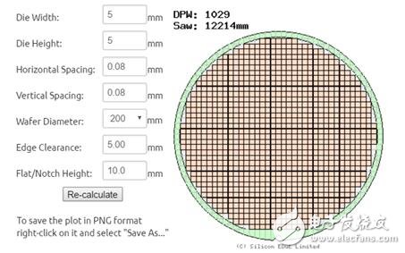
Organize your cabling