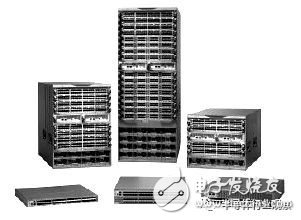
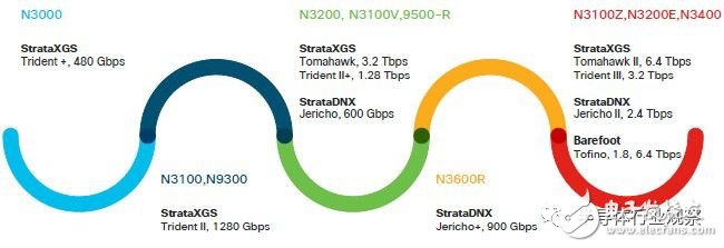
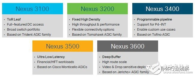
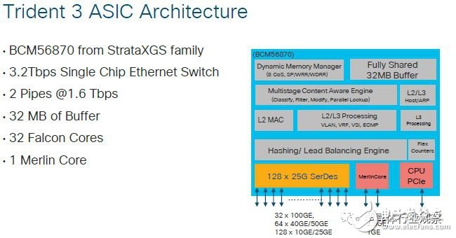
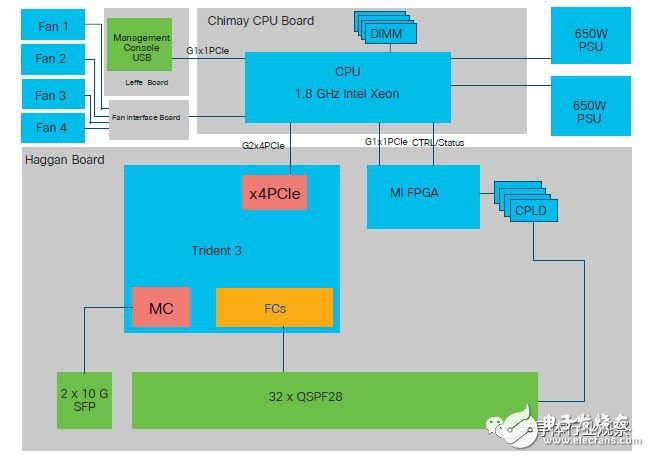
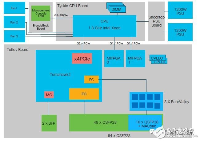
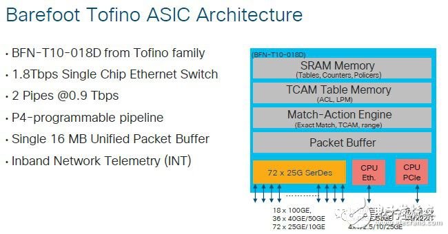
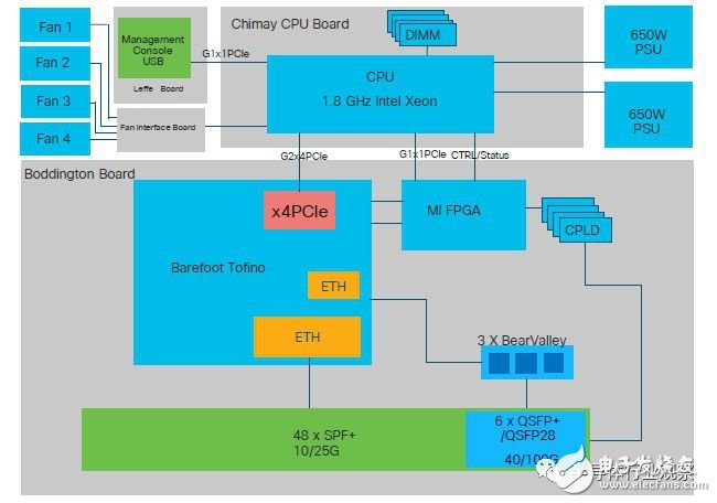
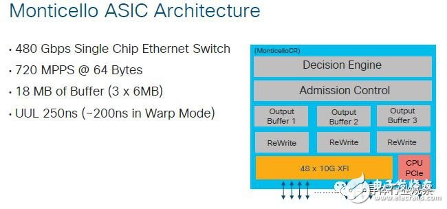
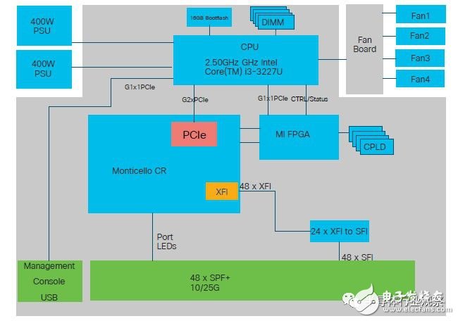
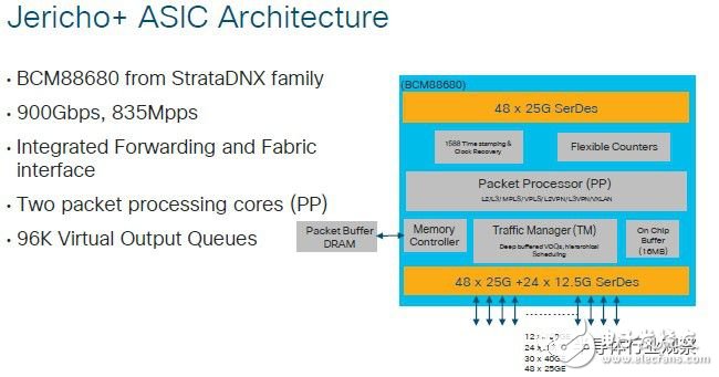
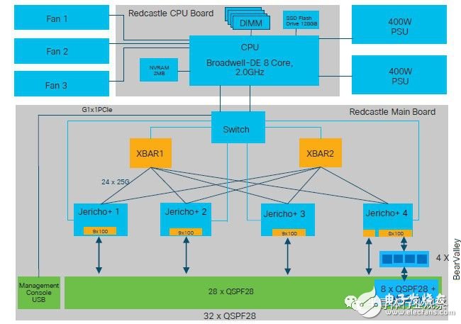
Existing switch manufacturers in the world can learn something from server rackets. In fact, they did. But this is because the world's ultra-large users and cloud builders have been advocating for them to decompose the components of the switch to open the switch architecture and promote them to make the device more programmable, so that they don't have to wait for years like today. The advent of a generation of chips. Throughout the development of the entire industry, in the past three decades, the Internet has become very commercialized, and the protocols and technologies of enterprise networks have changed. But we should also see that although the Ethernet and TCP / IP protocol stacks, which are the backbone of the Internet, are clearly open, the manufacturers of switching chips and switches are obsessed with internal components. Over the past few decades, they have also enjoyed the physical, psychological, technical, and economic thrill of this total control. We find this annoying, and for this reason we encourage leading switch chip manufacturers in the big data field (such as Broadcom, Mellanox Technologies, Barefoot, Cavium, and Innovium) to discuss their technologies in detail. But compared with the technology we obtained from global CPU manufacturers, their disclosed technology is too superficial. And the components of the switch are not as detailed as we can from any OEM or ODM server that we want to assemble. Perhaps one day, the exchange technology will become a reality. Recently, during the Cisco Live event hosted by data center switching equipment giant Cisco, we were particularly annoyed because we found that although Cisco has actually adopted Barefoot Networks' "Tofino" programmable switches, they did not want to admit this fact. Instead, it talks about its plans for future programmable switches, and hopes to re-enter the ultra-large-scale user data center and other things. But in fact, in addition to distributed fraud detection and risk analysis clusters in some financial services companies, Cisco does not have any other business in HPC, and the former is also market-based. Because they are familiar with iOS or NX-OS switch operating systems, they like to buy Cisco switch. Network administrators' familiarity with Cisco switch operating systems and different switch ASICs (whether developed independently or purchased from commercial switch chip suppliers) is the reason why Cisco still dominates the data center switch market. However, this share has dropped from 65% to about 50% during the Internet boom, for a reason. The most important point is that emerging switch manufacturers have adopted emerging commercial switching chips, changing the competitive landscape, pricing and pace of innovation in the market. But obviously starved to death, Cisco did not fight against them, but was forced to join their formation. Recently on Cisco Live, we found a beautiful demonstration made by Cisco technical marketing engineer Faraz TaifeshesmaTIan. Above, he detailed the commercial switching chips used in the Cisco Nexus 3000 series of top rack switches. It is worth mentioning that this series is a weapon against Cisco against white box switch manufacturers, as well as Arista Networks, Juniper Networks, Mellanox, Dell, HP from the Ethernet field. The PPT describes in detail and reflects the kind of openness we advocate. Although we cannot participate in Cisco Live, this is exactly what we want to see. Although TaifeshesmaTIan did not talk about the Nexus 9000 chip, as far as we know, the chip has "Alpine" and "Northstar" ASICs independently developed by Cisco, and its application center infrastructure (ACI) software-defined network expansion has been released. Even if he did not discuss in detail the switching chips used in commercial Nexus 9200, 9300 and 9500 switches. But the following chart does mention them: As you can see, in the past few years, Cisco has adopted a variety of Broadcom chips-Trident, Tomahawk, and Jericho series. Recently, the Nexus 3400 uses Tofino chips from Barefoot Networks. The following chart summarizes the target market and feature set of various Nexus 3000 switches: This is the wonder of the PPT summarized by TaifeshesmaTIan. It actually provides some chip technical details not disclosed by Broadcom and Barefoot. (Thank you sincerely.) Let's take them in order, starTIng with the Nexus 3000 family. The Nexus 3100 was based on Broadcom's “Trident-2†ASICs, which delivered 1.28 Tb / sec of aggregate bandwidth and had a 12.2 MB buffer. With the Nexus 3100-V, Cisco moved on up to the “Trident-2 +†ASIC, which boosted the buffer to 16 MB and had the same bandwidth. The Nexus 3100-Z adopted the “Trident-3†chip from Broadcom, which boosted the bandwidth by 2.5X to 3.2 Tb / sec and the buffer by 2X to 32 MB. Let's look at it in turn. The Nexus 3100 is based on Broadcom's "Trident-2" ASIC, provides a total bandwidth of 1.28Tb / sec, and has a 12.2MB buffer. On the new Nexus 3100-V, Cisco uses a new "Trident-2 +" ASIC, which increases the buffer to 16MB and has the same bandwidth. The Nexus 3100-Z uses Broadcom's "Trident-3" chip, which increases the bandwidth by 2.5 times to 3.2Tb / s and the buffer by 2 times to 32MB. The block diagram of the following Trident-3 chip: In this 1U switch, each of the 32 ports operating at 100Gb / sec has a "Falcon" core, and a 10Gb / sec "Merlin" core is used for management. The Trident-3 chip has two packet processing pipelines, and each pipeline has 16 Falcon cores, which are divided into two groups of Falcon SerDes. Every quarter of SerDes can access a quarter of the ASIC transmission bandwidth. The following figure is the actual application of Trident-3 in Nexus 3100-Z switch: As you can see, the switch itself is a hybrid server. On the board named "Chimay", it not only has Trident-3 ASIC, but also has a 1.8GHz Xeon processor with its own memory (we guess it is Intel's Xeon-D chip). In addition, an FPGA and a series of CPLDs are placed between the port and the FPGA to accelerate certain functions outside the switch chip. Observation shows that the Xeon processor is connected to the switch ASIC and FPGA through the PCI-Express link. Let's continue to look at the Nexus 3200. The product was originally designed based on Broadcom's "Tomahawk-2" ASIC, which has a total switching bandwidth of 3.2 Tb / sec, and has four 4MB buffer memories, totaling 16MB. The new Nexus 3200-E switch is also based on the Tomahawk-2 series, but it is rated at 6.4Tb / sec and has 4 pieces of 10.5MB buffer memory, totaling 42MB. This Nexus 3200-E adds a lot of functions, 64 ports based on 64 Falcon cores run at 100Gb / s, and a Merlin core is used for management, running at up to 100Gb / s. These ports can be divided into multiple slower ports, as shown in the block diagram. The structure of the Nexus 3200-E switch is as follows: Here is a different computing board called "Tyskie", which still has a 1.8 GHz Xeon CPU with its own memory slot. At first glance, this may be an upgraded version of the Xeon-D chip. In addition, the Nexus 3200-E has 48 Falcon cores, the port processing speed is 100Gb / s, and 16 ports have MACsec encryption, which is used to encrypt data when entering and exiting the switch. The chip also has two FPGAs for function acceleration. Interestingly, Cisco has not yet announced a switch based on Broadcom's "Tomahawk-3" chip design announced in January this year, but we guess it will be launched at the end of this year or early next year. We continue to watch the Nexus 3400. This is a new type of switch based on Barefoot Networks' Tofino programmable chip. Cisco announced the launch of the Tofino switch on the 3400 product line. Among them, 18 ports use 1.8Tb / sec entry-level Tofino ASIC, which runs at 100Gb / sec, but they also showed that it uses the high-end 6.4Tb / sec portion This means that a 64-port Nexus 3000 series switch is under development. The following figure is a fairly low-key implementation of the Barefoot series: These ports can be divided into 36 ports operating at 40 Gb / sec or 50 Gb / sec or 72 ports operating at 10 Gb / sec or 25Gb / sec. This is a problem for some service providers, hyperscale users and cloud builders. It is very important. Of course, there is a 100Gb / sec management port on the Tofino chip, which can be divided as needed. The chip is divided into two blocks, each with a speed of 900Gb / s, with a 16MB unified packet buffer, and of course, a pipeline. It can be fully programmed through the open source P4 language created by Barefoot Networks. The Nexus 3400 looks a lot like the Nexus 3100, with some "Bear Valley" MACsec encryption circuits added to some ports of the Nexus 3200. In fact, it looks like an ASIC with a slightly different port configuration. Please see: Now let's look at the Nexus 3500, which has been used in this field for 6 years and is based on Cisco's own "Monticello" ASIC. This Nexus 3500 is specifically designed for high-frequency trading applications. Although it only has 10Gb / s ports, the port-to-port hopping delay is as low as 250 nanoseconds, which is much lower than the 450 nanoseconds that a relatively fast Ethernet switch usually uses . The following figure is a block diagram of Monticello ASIC: The Monticello chip has three buffers, providing 18MB of capacity, and the packet transmission engine can provide an aggregate bandwidth of 480Gb / s, processing 720 million packets per second. Again, this is not big news, but delays, especially consistent delays, are the most important. The following figure is a block diagram of the Nexus 3548 switch: This switch exposes its age, but it may still be widely used in the financial services industry. As the only instance of the Nexus 3500, the Nexus 3548 uses Intel's dual-core "Ivy Bridge" Core i3-3227U processor, which can be overclocked from a rated speed of 1.9GHz to 2.5GHz. At the same time, the processor has 16 MB of built-in flash memory and can be booted from DRAM memory. In addition, the Nexus 3548 chassis has an FPGA that can support 48 ports running at 10Gb / s or 25Gb / s. The last point is very simple, because the 25G standard was released long after the 25G Ethernet standard was introduced. Obviously, there are some software-defined functions that work with Monticello ASIC. This is good. Finally, the Nexus 3600 series deep buffer switch based on Broadcom "Jericho +" ASIC. The original Nexus 3600 has a pair of Jericho + ASICs, which can provide 1.8 Tb / sec switching bandwidth, and has a buffer capacity of 8 GB (note that GB, not MB), while the second generation launched this year has four Jericho + chips , Switching bandwidth up to 3.6 Tb / s and buffer capacity of 16GB. The following figure is a block diagram of Broadcom Jericho ASIC: Each Jericho + chip can reach a bandwidth of 900 Gb / s, processing 8.35 million packets per second, and the chip has a pair of packet processing cores containing 96 virtual output queues. These packet buffers are based on GDDR5 memory and are the same as those used in graphics cards. Here is the architectural layout of the latest Nexus 3636 switch: The processor board on the switch is called "Redcastle", it is based on an 8-core Broadwell Xeon-D chip, running at 2GHz. The server board embedded in the switch has 2MB of NVRAM memory next to its DRAM main memory, and there is also a 128GB flash drive for booting the NX-OS network operating system. There is a PCI-Express switch that connects the CPU module to four Jericho chips. These four chips have their own crossbar circuits for connecting to each other. (In fact, this is a two-layer network in a chassis, just like a separate switch.) The Nexus 3636 switch has four Bear Valley chips on the board, and they are 8 of the 32 ports in the chassis Provides MACsec encryption. Military power supply is accordance with the relevant standard military standards. Linear DC Power Source,DC Power Source,Switching DC Power Source,Modular Power Supply Jinan Xinyuhua Energy Technology Co.,Ltd , https://www.xyhenergy.com