LED controllable constant current source drive system design
As the third-generation illumination source, LED has the advantages of low operating voltage, low power consumption, high luminous efficiency and long life. The LED is a non-linear device. When the LED is turned on, as long as the voltage on the LED changes slightly, the current will be too large and the LED device will be damaged. The working characteristics of LEDs depend on the quality of their power supply. Therefore, it is important to realize a high-quality power supply to improve the lighting quality, power utilization and extend the service life of LEDs. The stability of the power supply depends mainly on the LED driver circuit design. The constant current source driver is the best LED driver. It is driven by a constant current source. The current flowing through the LED will not be affected by voltage, ambient temperature, and discrete LED parameters. The effect is to keep the current constant and give full play to the various excellent characteristics of the LED. There are two forms of constant current sources widely used: one is a linear power supply improved constant current source, and the other is a switching power supply constant current source. The linear power supply improved constant current source has large linear loss and a small application range; the switching power supply constant current source has poor reliability, a small adaptation range, and high cost. Therefore, the economical, practical and reliable digital constant current source has been widely used. In view of some shortcomings of the driving method of small power LED in the existing lighting system, this paper designs an efficient driving system and proposes a corresponding new driving system.
1 LED characteristics
1.1 LED volt-ampere characteristics
The mathematical model of the volt-ampere characteristics of the LED can be expressed as:
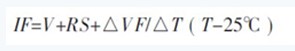
Where V is the LED starting voltage; RS is the volt-ampere curve slope; IF is the LED forward current; T is the ambient temperature; ΔVF/ΔT is the temperature coefficient of the LED forward voltage, for most LEDs, it A typical value is -2V/°C. From the mathematical model of the LED, a small change in the forward voltage of the LED after a forward conduction will cause a large change in the LED current under certain ambient temperature conditions.
1.2LED temperature characteristics
The magnitude of LED forward current varies with temperature. The operating current of white LED is generally about 200mA. When the ambient temperature exceeds 50°C, the allowable forward current of white LED will decrease and the normal luminance will not be achieved. The required operating current, in this case, if a large current is still applied, it is easy to age the white LED.
1.3 LED optical characteristics
The luminous flux of a light source refers to the visible light energy passing through a 4Ï€ solid angle per unit time. The relationship between white LED current and luminous flux is shown in Figure 1. As the current increases, the luminous flux of the LED increases nonlinearly and gradually becomes saturated. The reason is mainly because as the current and time increase, the internal temperature of the high-power LED rises, and the probability of carrier recombination occurring in the P/N junction region decreases, resulting in a decrease in LED luminous efficiency.
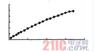
Figure 1 LED luminous flux and current diagram
2 System plan selection and comparison
2.1 system structure block diagram
The system structure block diagram is shown in Figure 2.

Figure 2 LED controllable constant current source drive system block diagram
2.2 Core Controller Selection
The controller adopts the current STC series single-chip microcomputer STC89C52, a high-performance 8-bit microprocessor with 8K bytes of flash programmable programmable read-only memory (FPEROM-Falsh Programmable and Erasable Read Only Memory). The device is fabricated using high-density nonvolatile memory fabrication technology and is compatible with the industry-standard MCS-51 instruction set and output pins. With a combination of a versatile 8-bit CPU and flash memory in a single chip, STC's STC89C52 is a highly efficient microcontroller that provides a flexible and cost-effective solution for many embedded control systems.
2.3 Clock function module selection
Option 1 uses the DS1302 clock chip. This chip is small in size, has few pins, and is very convenient to operate. The disadvantage is that an external backup battery and an external crystal oscillator are required for use, and the hardware circuit is complicated and the cost is high.
Option 2 uses the DS12C887 clock chip. The chip is relatively large in size and has a rechargeable lithium battery integrated therein. It also integrates a 32.768 kHz standard crystal oscillator, which can effectively maintain the continuity of time and is very convenient to use, but expensive.
Scheme 3 uses the timer of the microcontroller (crystal oscillator 11.0592M) to design the clock. The time is displayed on the 1602 LCD, and the hour, minute, and second of the clock are adjusted with a separate keyboard, and the timing can be set. The cost is low, no need to enable other chips and peripheral circuits, but the program is more complicated.
Consider the cost performance problem and the circuit optimization problem, so choose option 3.
2.4 constant current source module selection
Scheme 1 uses a single-chip microcomputer to generate a PWM signal, and the output reaches the Linton tube, and the ripple is eliminated by the filter to realize the constant current source function. The constant current source realized by PWM pulse mode can simplify the hardware circuit and is easy to control and adjust. However, the accuracy of the scheme is difficult to guarantee. It is technically difficult to adapt to the accuracy requirements of this design, and the scheme is difficult to adapt to current regulation. A wide range of application requirements, limited by ripple and stability, are difficult to achieve.
The scheme 2 constitutes a constant current circuit by an arithmetic V/I conversion circuit. The constant current circuit formed by the operational amplifier is free from the disadvantage that the transistor constant current circuit is limited by the process parameters. The scheme can realize V/I conversion of 0~5V/0~500mA, and the conversion precision is high. If the input terminal is controlled by a single-chip microcomputer with a digital potentiometer, it is also convenient to implement a digitally controlled constant current source.
Solution 3 implements a voltage-controlled current source solution through a dedicated constant current/constant voltage chip LT1769 and a simple control circuit. This constant voltage chip has the advantage of high integration, and the hardware and software used to control the system become relatively simple. However, the disadvantage is that the implementation of the scheme is not flexible; because the accuracy of the chip is not high, the performance of the device is limited to the range allowed by the performance index of the dedicated chip. Therefore, this design is generally only suitable for occasions where the precision requirements are not high, but the integration and portability requirements are high. It turns out that this is not an ideal implementation of the digitally controlled current source.
In view of the argumentation and comparison, the final choice is 2.
2.5D/A converter selection
For D/A converters, I use the very popular 8-bit D/A converter DAC0832 with a conversion time of 1μs, an operating voltage of +5V~+15V, and a reference voltage of ±10V, which is fully compatible with the microprocessor interface. It has the advantages of low price, simple interface, easy conversion control, etc., and is widely used in single-chip application systems. The D/A converter is composed of an 8-bit input latch, an 8-bit DAC register, an 8-bit D/A conversion circuit, and a conversion control circuit.
3 hardware circuit design
3.1 system power circuit
As shown in Figure 3, the power supply uses a positive-voltage integrated regulator LM7812 and a negative-voltage integrated regulator LM7912 to provide a symmetrical positive/negative 12V regulated output for use by the op amp, which is then regulated to a 5V output by the LM7805. Supply to the microcontroller.

Figure 3 system power circuit diagram
3.2 LED drive circuit
The circuit shown in Figure 4 can easily implement voltage/current conversion. The op amp U1A constitutes a comparator, and U1C constitutes a voltage follower, which acts as a negative feedback. The input signal Vi is compared with the feedback signal Vf. The output voltage V1 is obtained at the output of the comparator U1A. V1 controls the output voltage V2 of the operational amplifier U1B, thereby changing the output current IL of the transistor Q1, and the output IL affects the feedback voltage Vf. The purpose of tracking the input voltage Vi is reached. The output current IL is calculated as IL=Vf/R13, and negative feedback makes Vi=Vf, so IL=Vi/R13. If R13 is 10Ω, V~I conversion of 0~5V/0~500mA can be realized. If the performance parameters of the selected device are stable, the amplification factor of the operational amplifiers UA1 and UA2 is large enough, and the conversion accuracy is high. The voltage of V13 is controlled by the MCU with D/A output, which is convenient for digital constant current source output.
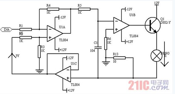
Figure 4 LED drive circuit diagram
3.3D/A conversion circuit
The DA conversion circuit is shown in Figure 5.
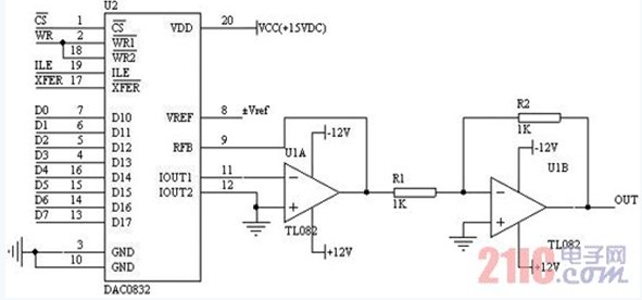
Figure 5D / A conversion schematic
4 software design
The tasks of the software system mainly include D/A conversion, step addition and subtraction, keyboard scanning, liquid crystal display, clock and other functions. In order to organize all tasks in an orderly manner, the software system adopts a front-back structure. Among them, the keyboard scanning and liquid crystal display are placed in the main program. The D/A conversion task needs to run in a fixed cycle and is placed in the time base interrupt service subroutine, which effectively ensures that important tasks can be executed in time.
The system adopts the watchdog technology. If the program has an infinite loop or runaway phenomenon, the internal watchdog of the microcontroller will reset the microcontroller and pull the microcontroller back to the ordered working state.
4.1 main program
After the system power-on reset, the main program first completes the system initialization, including I/O port, interrupt system, timer/counter and other working state settings, system variables and initial values.
After completing the system initialization, the interrupt is turned on, and then the keyboard scanning program is entered. After the keyboard scans to obtain the key value, the preset current value, step addition and subtraction, clock adjustment, etc. are completed according to the key value, and the output current value and time are displayed through the LCD. . The main program flow chart is shown in Figure 6.
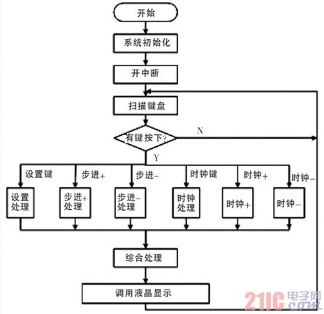
Figure 6 main program flow chart
4.2D/A conversion program
D/A Converter DAC08