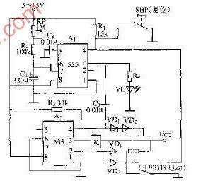
The following figure shows the 555 forming 5MIN startup delay circuit diagram, which uses two 555-time integrated circuits (the integrated circuit is a kind of micro-electronic device or component. Using a certain process, the transistors, diodes, resistors, etc. required in one circuit Components such as capacitors and inductors and wiring are interconnected and fabricated on a small or small piece of semiconductor wafer or dielectric substrate, and then packaged in a package to form a micro-structure with the required circuit functions) A1 and A2, A1 A monostable circuit is formed with the peripheral components; A2 is connected as a bistable circuit. Press the reset button SBP, A1 is set and output low level, the LED VL is off; press the start button SBT, the 3 pin of A2 outputs high level, and the relay loses power. A1 starts to delay. When the delay ends, A1's 3 pin outputs a trigger signal to the set end of A2 (4 pin), A2's 3 pin inputs low level, and K goods charge. At this point, the LED is bright, indicating that the monostable circuit has entered steady state. The time taken by VL from off to on is the start delay time, and the value of RP, R3 or C2 is adjusted to make the delay time suitable. The resistance value is shown below, and the delay time can be adjusted within 2~5min. 555 constitutes 5MIN startup delay circuit diagram Dongguan Yijia Optoelectronics Co., Ltd. , https://www.everbestlcdlcms.com