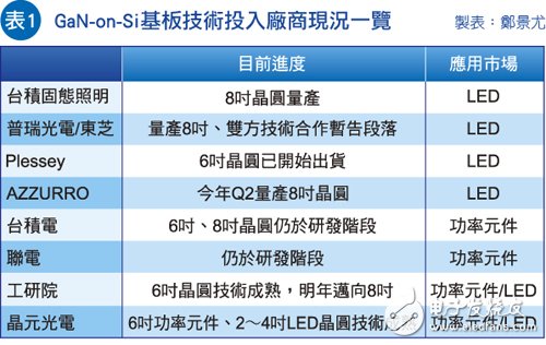
This year, the development of GaN-on-Si substrate market is freezing. At the end of May last year, Bridgelux and Toshiba announced that they have jointly developed a light-emitting diode (LED) chip based on 8-inch GaN-on-Si substrate technology. The device uses 350 milliamperes (mA) ) Current, the voltage is less than 3.1 volts (V), the size is only 1.1 mm, and the brightness can reach 614 milliwatts (mW). Unexpectedly, less than a year after this exciting news, Puri Optoelectronics and Toshiba announced at the end of April this year that Puri Optoelectronics will sell all its GaN-on-Si technology assets to Toshiba, both of which will The technical cooperation on the on-Si substrate will come to an end. This move is like throwing a powerful shock bomb in the industry. It is understood that in the latest agreement, Bridgelux will sell its GaN-on-Si technology and related assets to Toshiba. In the future, both parties will strengthen strategic technical cooperation through extended licensing and manufacturing relations. The procedures related to this asset transfer agreement were successfully completed at the end of May. Brad Bullington, CEO of Bridgelux Optoelectronics, said that Bridgelux Optoelectronics and Toshiba will jointly advance to the next milestone in GaN-on-Si substrate LED solid-state lighting technology. In the future, Bridgelux Optoelectronics will continue to promote the commercialization of GaN-on-Si technology. However, at the same time, Bridgelux will continue to develop sapphire LED substrate solutions to provide customers with higher standards and innovative services. Makoto Hideshima, Vice President of Toshiba Corporation and Executive Vice President of Semiconductors and Storage Products, believes that after the cooperation with Puri Optoelectronics enters a new stage, Toshiba can accelerate the mass production of 8-inch GaN-on-Si LED wafers. This move will allow The performance of the respective LED business departments of both parties continued to grow. Not only that, the GaN-on-Si technology obtained by Toshiba will also bring breakthroughs in the development and production of Toshiba power components. In response to the above news, Xie Mingxun, vice president of Epistar R & D Center, pointed out that the cooperation between Pree Optoelectronics and Toshiba is just like the investment trend of the epitaxial industry. Since GaN-on-Si technology breakthroughs will take a longer time, In terms of the current progress of the industry, it will take at least 3 years to enter the mature stage of mass production of large-sized substrates, so this news release is not surprising. In fact, the current market share of substrates in the LED lighting market is still dominated by sapphire substrates and silicon carbide (SiC) substrates. Although GaN-on-Si substrate technology has also risen rapidly in recent years, the current GaN-on-Si substrate yield rate In addition, there are several challenges to be solved. Tan Changlin, general manager of TSMC Solid State Lighting, analyzed the reason why GaN-on-Si substrates are just beginning to attract attention, that is, silicon materials are quite mature in semiconductor process technology, but in fact the GaN-on-Si substrates are bent during the growth process The situation does not apply to the existing wafer leveling equipment. Therefore, the investment in equipment for producing GaN-on-Si substrates is almost equivalent to investing in a new 8-inch factory, and the high investment number has become a hesitant for manufacturers to develop. Great cause. Not only that, the current large-scale LED epitaxial organic metal chemical vapor deposition (MOCVD) system has insufficient practical experience. AIXTRON launched the 8-inch production line version in the fourth quarter of last year, and the current 12-inch version is basically still The single-chip Solution belongs to the research and development (RD) stage of the epitaxy plant. It takes 1 to 2 years of testing time from the official operation and large-scale commercialization. On the other hand, because the silicon substrate itself has light absorption characteristics, in order to improve the luminous efficiency of the LED chip, most of the manufacturers will remove the silicon substrate after the epitaxy is generated, and a reflective layer must be added during the packaging step to enhance the overall brightness performance of the LED chip Therefore, whether the overall material cost can be significantly reduced is still full of many question marks. LED applications encounter technical bottlenecks, the industry turns to the power component market Xuan Rong, manager of the optoelectronic epitaxial component department of the optoelectronic components and system application group of the Institute of Electro-Optical Engineering of the Industrial Technology Research Institute, said that due to the high threshold of LED GaN-on-Si technology, several epitaxial factories have encountered major technical bottlenecks since the first half of this year. Coupled with the huge amount of investment in the GaN-on-Si substrate technology in the early stage, manufacturers will begin to change their investment strategies when they cannot reach a yield of more than 50%. Therefore, it is foreseeable that starting from the second half of this year, investment in GaN-on-Si substrates The number of technology epitaxy plants will decline rapidly. Xuanrong further analyzed that in terms of the cost structure of a single LED die (Single Die), the substrate, the epitaxy generation of the MOCVD system, and the wafer process accounted for 7%, 30%, and 63%, respectively. In order to make the cost of silicon substrates in 7% of the cost ratio show benefits, and widen the gap with sapphire (Sapphire) substrates, GaN-on-Si substrate manufacturers are targeting 8-inch wafer production, which is also epitaxial An important indicator for manufacturers to decide whether to continue investing. Xuanrong explained that in the current MOCVD machine area, regardless of the diameter of the wafer, 3 mm (mm) of uneven heating edges must be cut off. Therefore, if fourteen 4-inch wafers and eight 6-inch wafers are respectively Compared with the investment cost of a 56-inch 2-inch wafer system and a 56-inch 2-inch wafer system, the effective area of ​​a large-size wafer will be much larger. Taking the 5-chip 8-inch wafer solution as an example, due to its effectiveness The area is 74% more than the 2-inch solution, so you can get 58% of the system investment cost and get the same GaN-on-Si substrate benefits. In view of this, the industry is working hard to develop large-size GaN-on-Si substrates of 6-8 inches or even 12 inches. It is understood that the Institute of Optoelectronics of the Industrial Technology Research Institute is currently one of the few domestic research units that already has mature 6-inch GaN-on-Si substrate technology (Figure 3). The luminous efficiency of the GaN-on-Si substrate developed by it has reached the sapphire substrate solution. 70% of the GaN-on-Si substrate currently developed by Electro-Optics is close to the upper limit of the sapphire substrate solution-3.2 volts (V), and will be further reduced in the future. In order to improve the defect density of GaN film (Defect Density). Figure 1 The Institute of Industrial Technology has successfully developed a 6-inch GaN-on-Si substrate. Xuanrong revealed that although the GaN-on-Si substrate technology is difficult and there are multiple thresholds that must be further broken, resulting in a reduction in the number of manufacturers willing to invest, in the long run, compared to the current substrate technology, GaN-on-Si substrate The cost-effectiveness that can be brought to LED is still very predictable. Therefore, in the future, the electro-optical institute will continue to move towards mass production. After the luminous efficiency, yield and substrate size are expanded to 8 inches next year, the electro-optical institute will further move toward technology. Give Lei Jing Factory or set up a wholly-owned company. In addition to ITRI, TSMC, UMC, and Epistar have continued to invest in GaN-on-Si substrate technology. However, compared with the industry ’s optimistic attitude towards LED adoption of GaN-on-Si substrate technology last year, the attitude of manufacturers this year There is a substantial change. Xuanrong pointed out that because LEDs are similar to the GaN-on-Si substrate front-end epitaxial technology in the power component application market, in the trend of declining gross profit in the LED application market, manufacturers would rather target investment in emerging, high-margin orientation, and technology The market for power components with a lower threshold. Another major reason for the major policy change of manufacturers is that compared with GaN-on-Si substrate technology for LED applications, the power element GaN-on-Si has lower requirements for thin film defect density and eliminates the wavelength required for LED light emission. Technical threshold for uniformity. The most important thing is that the GaN thin film of the power element does not need to go through the silicon doping (Doping) process, and it is less difficult to grow on the silicon substrate. It is understood that at present, the Institute of Industrial Technology has developed GaN-on-Si substrates for 6-inch power components and LED lighting applications; TSMC has developed GaN-on-Si substrate technology for power component applications, and its subsidiary TSMC solid-state lighting is Responsible for LED application market; UMC invests most of its resources in the power component application market; Epistar Photonics is a leader in the LED epitaxial market, and is now actively developing power component GaN-on-Si substrate technology, hoping to take this opportunity The new application market (Table 1). When the future of GaN-on-Si substrate LEDs is not clear, a new wave of substrate technology-GaN-on-GaN substrate (GaN-on-GaN) LEDs is gradually gaining momentum. GaN-on-Si traps GaN-on-GaN substrates GaN-on-GaN substrates do not need to overcome the lattice and thermal expansion coefficients that are a headache for GaN-on-Si substrate LED developers. Coupled with the breakthroughs in GaN substrate technology, the price decline can be expected, so it has gradually become a high-profile LED Substrate alternatives. In view of this, the industry has turned its attention to other more cost-effective alternatives, among which GaN-on-GaN substrates have received considerable market attention in the near future. At present, the US startup Soraa is the main developer of the substrate technology, and it officially announced a technological breakthrough in February this year. Compared with GaN-on-Si substrates, GaN-on-GaN substrates do not have the problems of thermal expansion coefficient mismatch (CTE Mismatch) and lattice mismatch (LatTIce Mismatch), and because the density of lattice defects is extremely low, LED chips can be made Operates at a very high current density and emits more than ten times the brightness per unit area compared to traditional substrate solutions such as sapphire, silicon carbide, and silicon. Despite this, the current price of GaN-on-GaN substrates is still high, about ten to fifteen times that of sapphire substrates. Therefore, its application is still dominated by niche markets, such as the automotive lighting market that requires high brightness. Tan Changlin pointed out that a few days ago Soitec has published Smart Cut technology for GaN substrates and transferred the technology authorization and technology to Sumitomo Electric. This move is expected to accelerate the decline of GaN substrate prices. It is understood that Soitec and Sumitomo Electric have previously used the technology to successfully trial-produce 4-inch and 6-inch GaN substrates. This process technology has enabled high-quality, ultra-fine GaN layers to be repeatedly converted from a single wafer to multiple substrates. The results show that with the help of Smart Cut technology, GaN substrates can exhibit high performance and maintain low cost. Therefore, Sumitomo Electric will continue to invest in Smart Cut technology in the future and use this technology to manufacture larger GaN substrates. Tan Changlin believes that in the future, the materials and technologies of substrates such as sapphire, silicon carbide, GaN, and silicon will continue to be integrated, and the improvement of luminous efficiency (lm / w) and declining light efficiency (Droop) and manufacturing costs will determine the layout of substrate power Key factor. No matter which substrate technology will become mainstream in the LED market in the future, LED brightness and cost will have further breakthroughs and bring good news to the LED lighting market. Pv Module,Solar Pv Module,Pv Module Solar Panel,Solar Panel Tier TRANCHART Electrical and Machinery Co.,LTD , https://www.tranchart-electrical.com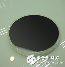
![]()