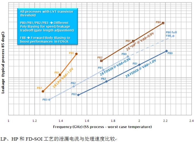
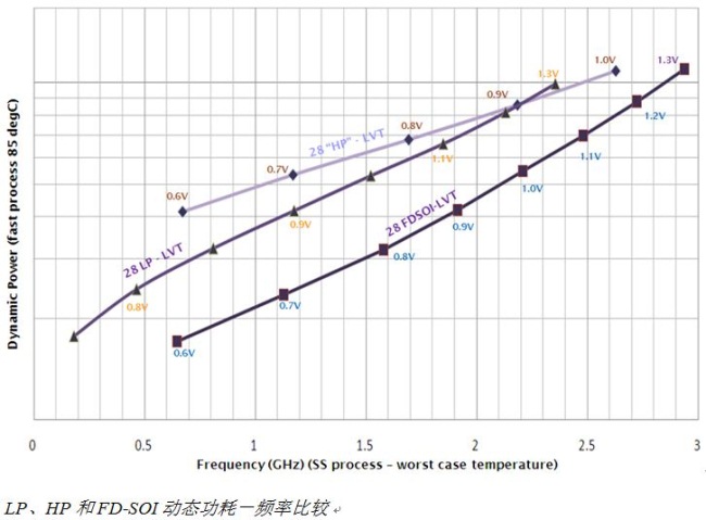
As smartphone functions have recently evolved and evolved, consumer expectations are rising. Faster multi-core, high-frequency CPU processors, stunning 3D graphics, full HD multimedia and high-speed broadband are now standard on high-end phones. At the same time, consumers also expect the phone to be slim and light, and the battery life is at least equal to the previous phone. For mobile phone manufacturers and designers, consumer expectations mean that mobile chips need to have superior performance while at the same time providing low cost and low power consumption. FD-SOI (Fully Depleted Silicon on Insulator) is the best solution to meet these needs. This article refers to the address: http:// At the Mobile World Congress in 2012, Idea-Ericsson CEO Didier Lamouche confirmed that our next-generation NovaThor platform, the successor to the NovaThorL8540, will use the 28nm FD-SOI manufacturing process. FD-SOI technology is currently available for chip development, which will significantly improve the performance and power consumption of 28nm process chip products. Because of the relatively low process complexity, FD-SOI solves problems such as process upgrades, leakage currents, and variability, and can further reduce CMOS process nodes to 28 nm or less. Like FinFET technology, FD-SOI was originally developed for 20nm nodes and below, which can overcome the limitations of traditional body-effect CMOS process upgrades, such as high leakage current and terminal device diversity; however, with FinFET technology Differently, FD-SOI retains the advantages of relatively low planar structure complexity of conventional bulk CMOS processes, which speeds up process development and mass production, and reduces the migration difficulty of existing designs. The technical cooperation between ST-Ericsson, STMicroelectronics, Leti and Soitec allows us to take advantage of FD-SOI at 28nm technology nodes: advanced performance, competitive processing speed/leakage current ratio and optimized energy efficiency. The first part of the article focuses on performance, and the second part discusses the other two advantages. Leading performance over a wide voltage range The graph below compares the highest frequency-Vdd supply voltage curve that can be achieved with a particular critical channel of the ARM Cortex-A9 CPU core at the slowest process angle (SS) and ambient temperature. Each curve represents a specific 28nm process: The 28HP-LVT is a high-performance body-effect CMOS process for mobile devices that targets high-performance mobile device CPUs with fast processing speed and thin gate oxide. Therefore, Vdd has limited drive capability due to reliability. ~1.0V). The 28LP-LVT is a low-power, bulk-effect CMOS process that has been used in low-power mobile applications in the past. LPs are based on thicker gate oxide transistors and support higher overdrive voltages (up to 1.3V). The 28FDSOI-LVT is a 28nm FD-SOI process developed by STMicroelectronics. The gate structure is similar to that of the 28LP and also supports a 1.3V overdrive voltage. Of these three processes, only the low voltage threshold (LVT) is considered because the processing performance is highest at such voltages. 1. First observed, at the nominal voltage (HP = 0.9V, LP = 1.0V, FD-SOI = 1.0V), the peak performance of FD-SOI is similar to the HP process; when the Vdd voltage is the same, performance 35% higher than LP. 2. In addition, as the Vdd voltage increases, the performance of the FD-SOI is further improved, and the HP process cannot withstand higher voltages. Therefore, the integrated peak performance of the former is higher than the latter. 3. When the working voltage is too low, such as Vdd=0.6V, LP will not operate or performance is very low; FD-SOI is equivalent to HP process even higher than HP process, but the former leakage current and dynamic power consumption are better than the latter A lot lower, I will give a description in the following content. 4. Compared to bulk CMOS technology, FD-SOI has low process variability and can support lower operating voltage (minimum 0.5V) when it is suitable for CPU processing non-intensive tasks (200MHz-300MHz). For example, Hardware acceleration sound, video playback. Therefore, in the wide Vdd voltage range (0.5V to 1.3V), the overall performance of the FD-SOI is higher than that of the mobile processor-specific bulk CMOS process. These performance advantages can be used to improve peak performance or to ensure performance. Reduce the Vdd operating voltage to reduce dynamic power consumption. FD-SOI: Booster for the Next Generation NovaThor Platform (Part 2) In the previous section, we explored the technical advantages of the FD-SOI process in terms of performance-to-voltage ratio. Next, we will analyze two other advantages: competitive processing speed/leakage current ratio and optimized energy efficiency. Competitive processing speed / leakage current ratio The FD-SOI process not only brings the performance advantages described above, but also has the lowest leakage current of the same class. The figure below shows the typical leakage current and maximum frequency of the ARM Cortex-A9 critical channel at 85 °C. ratio. Systematic analysis, when the leakage current is the same, the operating frequency of the FD-SOI at the nominal voltage (1.0V) is higher than the LP process or the nominal voltage (0.9V) at the nominal voltage (1.0V). HP process. The light blue curve represents the FD-SOI leakage current/speed curve at Vdd = 0.9V, which means that FD-SOI allows us to lower the nominal Vdd voltage (a parameter that has a large impact on dynamic power consumption) while maintaining Same or higher performance than the HP process. Then, as indicated by the blue extended dashed line, the forward body bias (*) applied to the LVT FD-SOI transistor enables it to achieve HP's achievable performance, and the leakage current of the polysilicon transistor increases after the bias is applied. Same as the LP process. This leakage current/speed ratio advantage is unique to the 28nm FD-SOI process, truly combining the advantages of both LP and HP processes. Body bias is the application of a variable voltage in the body effect portion of a CMOS transistor to increase the leakage current at the expense of faster operating speed (forward body bias) or at the expense of performance for lower leakage current (reverse) Body bias). Although bulk CMOS has this function, the bulk bias effect is superior to FD-SOI technology because the buried oxide layer isolates the transistor channel from the silicon body effect portion (back gate effect). Optimize energy efficiency For high-end mobile applications, good processing performance and excellent leakage current are not enough. Reducing the total power consumption of different operating modes during the daily use of mobile devices is the key to maximizing battery life. The following figure depicts the dynamic power consumption characteristics of three different 28nm processes and gives the dynamic power-maximum frequency characteristic curve. It is easy to see from the figure that at a given frequency, the total power consumption of the FD-SOI is always much lower than the other two technologies, even if the power supply voltage required to reach the target frequency is slightly higher than 28 nm HP. This is mainly due to the lower leakage current in the total power consumption of the FD-SOI technology. This is true across the entire supply voltage range and the corresponding performance range, which fully demonstrates that FD-SOI is the solution that delivers the highest energy efficiency for mobile devices. As can be seen from the above, 28nm FD-SOI is superior to the existing body effect process in key parameters that are extremely important for mobile computing devices, and has the advantages of high performance and low power consumption. Therefore, ST-Ericsson selects FD- SOI designs the next generation NovaThor high-performance smartphone and tablet platform. The bimetal thermometer combines two metals with different linear expansion coefficients, and one end is fixed. When the temperature changes, the two metals have different thermal expansion, which drives the pointer to deflect to indicate the temperature.
WSS series bimetal thermometer is a kind of field measuring instrument for measuring medium and low temperature. It can directly measure the temperature of liquid, steam and gas medium in the range of - 80 ℃~+500 ℃ in various production processes. It is suitable for temperature measurement when the precision is not high in industry. As a temperature sensing element, bimetallic sheet can also be used for automatic temperature control.
The bimetallic thermometer can be divided into axial, radial, 135 ° and universal types according to the connection direction of the pointer plate of the bimetallic thermometer and the protective tube. Bimetal Thermometer,Explosion Proof Thermometers,Pointer Bimetal Thermometer,Boiler Pipes Pointer Thermometer Henan New Electric Power Co.,Ltd. , https://www.newelectricpower.com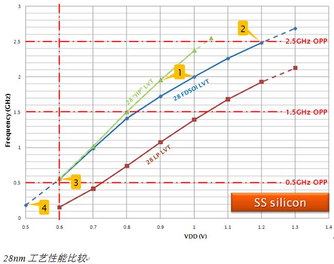
â‘ Axial bimetal thermometer: the pointer plate is vertically connected with the protective tube.
â‘¡ Radial bimetal thermometer: the pointer plate is connected with the protective tube in parallel.
③ 135 ° directional bimetal thermometer: the pointer plate is connected with the protective tube at 135 °.
â‘£ Universal bimetal thermometer: the connecting angle between the pointer plate and the protective tube can be adjusted at will.