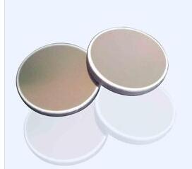
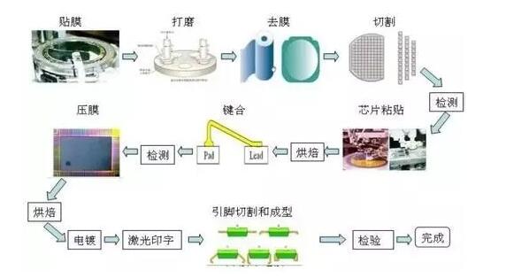
Semiconductor chip packaging refers to the use of membrane technology and micro-machining technology, the chip and other elements in the frame or the substrate layout paste and fixed and connected, leading out the terminals and the plastic insulating dielectric potting and fixed to form the overall three-dimensional structure of the process. This concept is narrowly defined package. A more generalized package refers to a package project, which connects and fixes the package body to the substrate, assembles a complete system or electronic device, and ensures the overall performance of the entire system. Combining the previous two definitions forms a generalized encapsulation concept. 1, protection Semiconductor chip production plants have very strict control of production conditions, constant temperature (230 ± 3*C), constant humidity (50 ± 10%), and strict air dust particle size control (usually between 1K and 10K). And strict static protection measures, exposed bare chips will not fail under this strict environmental control. However, the surrounding environment we live in is completely impossible to have such conditions, there may be -40^C in low temperature, 60*C in high temperature, and humidity may reach 100%. If it is an automotive product, its operating temperature may be as high as 120 ^C Above, in order to protect the chip, so we need to package. 2, support The support has two functions. One is to support the chip, the chip is fixed to facilitate the connection of the circuit, and the second is that after the package is completed, a certain shape is formed to support the entire device, so that the entire device is not easily damaged. 3, connection The role of the connection is to connect the electrodes of the chip with the circuits of the outside world. The pins are used to communicate with the outside world, and the gold wires connect the pins to the circuit of the chip. The slide table is used to carry the chip, the epoxy adhesive is used to attach the chip on the slide table, the pins are used to support the entire device, and the plastic seal body is used for fixing and protection. 4, reliability Any package needs to have a certain degree of reliability, which is the most important measure of the entire packaging process. The original chip will be destroyed after leaving a specific living environment and needs to be packaged. The working life of a chip depends mainly on the choice of packaging materials and packaging processes. 1. The process flow of packaging can generally be divided into two parts. The process steps before plastic encapsulation become the first stage operation, and the process steps after molding become the latter stage operations. 2. The basic process flow of chip packaging technology: wafer thinning, silicon cutting, chip mounting, chip interconnection molding, deflashing, burr, rib formation, soldering, and other processes 3. The backside thinning technology of silicon wafers includes grinding, grinding, chemical mechanical polishing, dry polishing, electrochemical etching, wet etching, plasma enhanced chemical etching, atmospheric plasma etching, etc. 4. Thinning after scribe: Before the back grinding, cut the front of the wafer to a certain depth of cut, and then back grinding. 5, thinning dicing: Before thinning, first cut the incision in a mechanical or chemical way, and then use ADPE corrosion technology to reduce the remaining processing volume after grinding to a certain thickness to achieve automatic separation of bare chips. 6, chip placement four ways: eutectic paste method, welding paste method, conductive adhesive paste method, and glass paste method. Co-crystallization paste method: Using a gold-silicon alloy (generally 69% Au, 31% Si), the eutectic fusion reaction at 363 degrees causes the IC chip to be stuck and fixed. 7. In order to obtain the best eutectic placement method, the back of the IC chip is usually plated with a gold film or implanted on the chip carrier of the substrate. 8. Common methods for chip interconnection include wire bonding, automatic bonding (TAB) and flip chip bonding. 9, wire bonding technology, ultrasonic bonding, hot-press bonding, thermal ultrasonic bonding. 10, TAB's key technologies: 1 chip bump production technology 2 TAB carrier tape production technology 3 with lead and chip bumps of the inner lead welding and carrier tape outside the wire welding technology. 11. Manufacturing process of bump chips, technology for forming bumps: evaporation/sputtering, dot plating, plating bump making, ball and stencil printing, solder bumps, chemical plating dots, playing convex Point production method, laser method. 12. Molding technology of plastic packaging, 1 transfer molding technology, 2 injection molding technology, 3 pre-molding technology but the most important technology is transfer molding technology, and the material used for transfer technology is generally thermosetting polymer. 13. The thinned chip has the following advantages: 1. The thin chip is more conducive to heat dissipation; 2. The volume of the chip package is reduced; 3. The mechanical properties are improved, the thinning of the silicon chip is better, and the flexibility thereof is better, which is caused by external impact. The smaller the stress is; 4, the thinner the wafer, the shorter the connection between components, the lower the on-resistance of the component, the shorter the signal delay time, thus achieving higher performance; 5, reduce the dicing Cutting the amount of processing after cutting it can reduce the amount of processing and reduce the incidence of chip disintegration. 14. Wave soldering: The wave soldering process includes fluxing, preheating, and passing the PCB board on a solder crest, relying on the joint action of surface tension and capillary phenomena to bring the solder to the PCB board and component pins. Form welding points. Wave soldering is the use of a molten solder in a molten liquid solder to form solder waves of a specific shape in the surface of the solder bath. The component-mounted PCB is placed on the conveyor chain at a specific angle and a certain depth of penetration. Through the solder peaks to achieve solder joint welding process. Reflow soldering: By applying appropriate and appropriate solder on the soldered area of ​​the PCB in advance, and then placing the surface mount components, and then remelting the solder paste pre-assigned on the printed circuit board pad to achieve surface mount component soldering A group or point-by-point soldering process of mechanical and electrical connections between terminals or pins and PCB lands. 15, wire bonding (WB): The thin metal wire or metal band in order to play on the chip and the lead frame or the packaging substrate pad to form a circuit interconnection. Wire bonding technology has ultrasonic bonding, hot-press bonding, and hot ultrasonic bonding. Tape Automated Bonding (TAB): A process of connecting a die pad with an I/O on an electronic package or a metal pad on a substrate with a lead patterned metal foil. Flip Chip Bonding (FCB): A method in which the chip surface is facing down and the die pad area is directly interconnected with the substrate pad area. 16. Chip interconnection: The chip soldering zone is connected with the I/O of the electronic package or the metal wiring pad on the substrate. Only the circuit connection between the chip and the package structure can be used to play the existing function.
What`s the main features appear into your mind when you look yoga laptop? Lightweight, super thinner, touch screen, 360 rotating, smaller size, like as notebook? You are right, that`s the main reasons why some people also called it as laptop yoga slim or yoga notebook. To OS, just same as Education Laptop-windows operating system, so you can see many windows yoga laptop at the market around the world. In fact, this intel yoga laptop usually is designed for normal jobs, like basic WPS, Photoshop, video or music editing, online learning, shopping, presentation when on a business trip, etc. At our store, you can see 11.6 inch n5100 360 Laptop in metal, 13.3 inch 360 flip laptop, and 14 inch 360 degree rotating laptop, etc. The people who take business trips often or prefer fashion design should like this type device.
There are education laptop also, like 14.1 inch Student Laptop for Hope or government Projects, 15.6 inch competitive celeron business laptop for normal business works, 15 inch 10th or 11th Gaming Laptop for heavier tasks, like teachers, high or university students, etc, 16.1 inch i7 16gb ram 4gb graphics laptop for engineering student, etc
Any other question or other requirements, just contact us freely.
Yoga Laptop,Laptop Yoga Slim,Yoga Notebook,Intel Yoga Laptop,Windows Yoga Laptop Henan Shuyi Electronics Co., Ltd. , https://www.shuyioemminipc.com