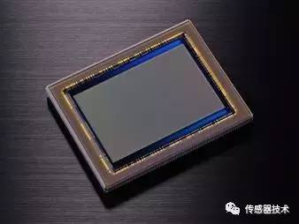
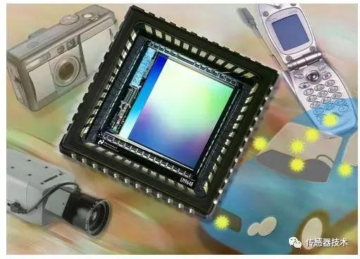
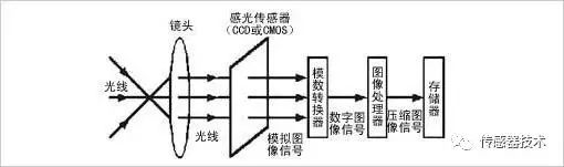
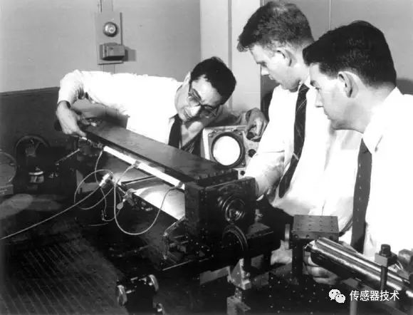
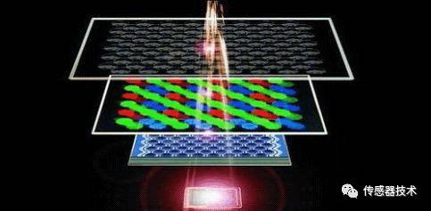
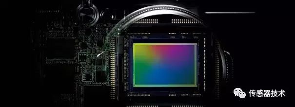
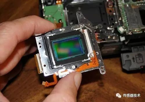
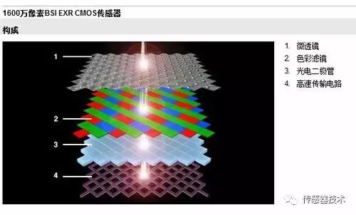
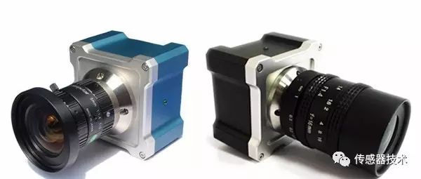
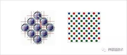
Image Sensors are the core components of various industrial and surveillance cameras, portable VCRs, digital cameras, scanners, etc. At present, this fast-growing market has now extended to the fields of toys, mobile phones, PDAs, automobiles, and biology. Image Sensor Definition and types of image sensors Image sensor application The imaging objective lens images the scene illuminated by the external illumination light (or self-luminous) on the image surface of the objective lens to form a two-dimensional light intensity distribution (optical image). A sensor that can convert a two-dimensional light intensity distribution optical image into a one-dimensional time series electrical signal is called an image sensor. The image sensor is an important part of the digital camera. According to the different components, image sensors can generally be divided into CCD (Charge-Coupled Device) and CMOS (Complementary Metal-Oxide Semiconductor) two categories. In addition to the above two common types, there is also a CIS (abbreviation for Contact Image Sensor, contact image sensor), which is generally used in scanners. Because it is a contact scan (it must be kept close to the original), only LED light sources can be used. Its depth of field, resolution and color performance are currently not as good as CCD photosensitive devices, nor can it be used for scanning transmissive films. Contact CIS With the rapid development of solid-state imaging applications in the 1970s and 1980s, CCD technology and manufacturing have been optimized in terms of optical characteristics and imaging quality. In the 25 years at the end of the last century, CCD technology has been dominating the trend of image sensor devices. It is a high-resolution and high-quality image sensor that can be integrated on a small chip. The CMOS image sensor has been developed rapidly in recent years, and it is very likely to come from behind. CMOS provides performance comparable to CCD in mid-range and low-end applications, and it does have a clear advantage in price. With the development of technology, CMOS will also occupy a place in high-end applications. How the image sensor works How the image sensor works The image sensor is a semiconductor device that can convert optical images into digital signals. The tiny photosensitive substances implanted on the sensor are called pixels. The more pixels contained in a sensor, the higher the picture resolution it provides. It acts like film, but it converts image pixels into digital signals. Development history and characteristics of CCD and CMOS CCD was invented in 1969 by Willard S. Boyle and George E. Smith of Bell Labs. Bell Labs At that time, Bell Labs was developing video phones and semiconductor bubble memory. After combining these two new technologies, Boyle and Smith came up with a device, which they named "Charge "Bubble" Devices. The characteristic of this device is that it can transfer electric charge along the surface of a piece of semiconductor, and it was tried to be used as a memory device. At that time, it could only input the memory by "injecting" electric charge from the register. But then it was discovered that the photoelectric effect can generate charges on the surface of such devices to form digital images. By the 1970s, Bell Labs researchers were able to capture images with simple linear devices, and CCD was born. CCD is still widely used in digital cameras and astronomy. We all know that CCD is a medium that replaces traditional film in the digital age, and its working principle is also evolved by the light-sensing principle of chemical substances on the original film. It is made of a high-sensitivity semiconductor material, which can convert light into electric charge, which is converted into a digital signal through an analog-to-digital converter chip. After being compressed, the digital signal is stored in the camera's internal flash memory or built-in hard disk card. You can easily transfer the data to the computer, and use the computer's processing means to modify the image as needed. CCD is composed of many photosensitive units, usually in megapixels. When the CCD surface is illuminated by light, each photosensitive unit will reflect the charge on the component, and the signals generated by all the photosensitive units are added together to form a complete picture. The more notable features of CCD are: 1. Mature technology 2. High imaging quality 3. High sensitivity, low noise, large dynamic range; 4. Fast response speed, self-scanning function, small image distortion and no afterimage; 5. It is produced by VLSI process technology, with high pixel integration and precise size. There are many indicators for evaluating the quality of a CCD sensor, such as the number of pixels, CCD size, signal-to-noise ratio and so on. The number of pixels and the size of the CCD are the most important indicators. The number of pixels refers to the number of photosensitive elements on the CCD. We can understand the picture we take as consisting of many small dots, each dot is a pixel. Obviously, the more pixels there are, the clearer the picture will be. If the CCD does not have enough pixels, the sharpness of the picture will be greatly affected. Therefore, the number of CCD pixels should be as large as possible. However, increasing the number of CCD pixels in order to get better picture quality will inevitably lead to a problem, that is, the increase in CCD manufacturing costs and the decrease in yield. Therefore, in view of a series of issues such as cost, a CMOS sensor with lower cost, lower power consumption and high integration has been born. CMOS is an important chip in the computer system, which saves the most basic information for system booting. CMOS The manufacturing technology of CMOS is no different from that of general computer chips. It mainly uses semiconductors made of the two elements of silicon and germanium, so that a negatively charged N-pole and a positively charged P-pole semiconductor coexist on the CMOS. The current generated by the two complementary effects of one positive and one negative can be recorded by the processing chip and converted into an image. It was later discovered that CMOS can also be used as an image sensor in digital photography after processing. CMOS CMOS image sensor is a typical solid-state imaging sensor, which shares a common historical origin with CCD. CMOS image sensor is usually composed of image sensitive unit array, row driver, column driver, timing control logic, AD converter, data bus output interface, control interface, etc. These parts are usually integrated on the same silicon chip. The working process can generally be divided into reset, photoelectric conversion, integration, and readout. The photoelectric information conversion function of CMOS is basically similar to that of CCD. The difference lies in the way of information transmission after photoelectric conversion of these two sensors. CMOS composition CMOS has the characteristics of simple way to read information, fast output information rate, low power consumption (only about 1/10 of CCD chip), small size, light weight, high integration and low price. It is precisely considering that the production cost and yield of CMOS sensors are higher than that of CCD sensors, so several well-known manufacturers have increased the research and development of CMOS sensors since 2000. The current growth rate of CMOS has reached several times. At the level of CCD. We can see that even in the early days of Nikon’s digital SLR products, there will still be some models of cameras using CCD sensors, but whether it’s Nikon, Sony or Canon’s digital cameras launched in recent years, it’s hard for us. See the CCD again. Although the use of CMOS sensors will save the cost of the camera, the image quality is still the most important for the camera. Compared with CCD, the biggest fatal injury of CMOS is the image quality. This is because the early CMOS has an obvious shortcoming. That is, the frequency becomes faster when the current changes, so heat will inevitably be generated, and eventually noise will appear on the picture and affect the image quality. If you compare CCD and CMOS sensors, the biggest advantage of CCD sensor is its high imaging quality, while the biggest advantage of CMOS is its low cost and easy mass production. The disadvantages of CMOS are constantly being improved. . At present, some medium-format digital cameras or digital backs still use CCD sensors. This is because different products have different requirements for image quality, so the price of those medium-format digital products is often much higher than that of ordinary digital cameras. Therefore, it can be said that the main development direction of the future camera market will still be CMOS as the core, and on this basis, the resolution and sensitivity of CMOS will continue to be improved. industrial camera The times are advancing, and cost saving is the business rule that every business is insisting on. The future of CCD is not necessarily in the camera market. In other fields, CCD will also be widely used with its own advantages. With the continuous development of science and technology, I believe that some day in the future, more types of sensors will appear. It is only a matter of time. At that time, we will look back to the past and see the film era, CCD era and In the CMOS era, I will sincerely lament the rapid development of science and technology. Comparison of CCD and CMOS 1. The imaging process CCD and CMOS use the same photosensitive material, so the basic principle of generating electrons after receiving light is the same, but the reading process is different: CCD is transferred in a frame or line mode under the cooperation of a synchronization signal and a clock signal. The entire circuit is very complicated. The output rate is slow; CMOS reads signals in a similar manner to DRAM, with simple circuits and high read rates. 2. Integration The CCD readout circuit with special technology is more complicated, and it is difficult to integrate A/D conversion, signal processing, automatic gain control, precision amplification and storage functions on a single chip. Generally, 3 to 8 chips are needed to realize the combination. A multi-channel non-standard supply voltage. With the aid of a large-scale integrated manufacturing process, CMOS image sensors can easily integrate the above-mentioned functions on a single chip. Most CMOS image sensors have both analog and digital output signals. 3. Power, power consumption and volume CCD needs a variety of power supplies, power consumption is relatively large, and the volume is relatively large. CMOS only needs a single power supply (3V~5V) to supply power, its power consumption is equivalent to 1/10 of CCD, and the highly integrated CMOS chip can be made quite small. 4. Performance indicators CCD technology is quite mature, and CMOS is in a period of vigorous development. Although the current high-end CMOS image quality is temporarily not as good as CCD, some indicators (such as transmission rate, etc.) have exceeded CCD. Due to the many advantages of CMOS, many institutions at home and abroad have developed many products using CMOS image sensors. Six hardware technical indicators of CCD and CMOS image sensors Sometimes people may have this question, why are the image effects of the same high-definition network camera different? Why is the effect different at night with the same Accessories? In fact, this is related to the hardware technical indicators of the sensor (ie image sensor) we use. Whether it is a CCD or CMOS image sensor, it mainly includes "pixels, target size, sensitivity, electronic shutter, frame rate, signal-to-noise ratio" These six hardware technical indicators. Pixels: There are many photosensitive units on the sensor, which can convert light into electric charges to form an electronic image corresponding to the scene. In the sensor, each photosensitive unit corresponds to a pixel (Pixels), the more pixels, it means that it can sense more object details, so that the image is clearer, and the higher the pixel, the clearer the imaging effect. Pixel Associated with our products of Zhongwei Century: 100W network camera resolution is 1280X720, the pixel value obtained by multiplying the two values ​​is nearly 1 million pixels, the resolution of 130W is 1280X960, and the pixel value is nearly 1.3 million Pixels. From the image effect point of view, the effect of 130W is better than that of 100W. Target size: The size of the photosensitive part of the image sensor is generally expressed in inches. Like a TV, this data usually refers to the diagonal length of the image sensor. For example, it is 1/3 inch. The larger the target surface, the better the light flux. The smaller the target surface, the easier it is to obtain. Greater depth of field. For example, 1/2 inch can have a relatively large amount of light, while 1/4 inch can easily obtain a larger depth of field. "Relate to our Zhongwei Century products: 100W products are 1/4 inches, 130W is 1/3 inches, and 200W is 1/2.7 inches. You can perceive the different sizes of the target surface mentioned above from the screen. The image quality changes come. Sensitivity: That is, the intensity of incident light is sensed through CCD or CMOS and related electronic circuits. The higher the sensitivity, the stronger the sensitivity of the photosensitive surface to light, and the higher the shutter speed. This is especially important when shooting moving vehicles and monitoring at night. This explains why the night vision of different cameras is very different. The unit of sensitivity is V/LUX-SEC, V (volt) is the unit of voltage we usually say, LUX-SEC: the unit of light intensity , The greater the ratio, the better the night vision effect. Electronic shutter: It is a term referring to the mechanical shutter function of a camera. It controls the light-sensing time of the image sensor. Since the light-sensitivity value of the image sensor is the accumulation of signal charge, the longer the light-sensitivity, the longer the signal charge accumulation time, and the greater the amplitude of the output signal current. The faster the electronic shutter, the lower the sensitivity, which is suitable for shooting under strong light. Frame rate: It refers to the number of pictures recorded or played per unit time. Continuously playing a series of pictures will produce animation effects. According to the human visual system, when the picture playback speed is greater than 15 frames per second (that is, 15 frames), the human eye can hardly see the jump of the picture; when it reaches 24 frames /s ~ 30 frames/s (that is, between 24 frames and 30 frames), the flicker is basically not noticeable. The number of frames per second (fps) or frame rate indicates the number of times the graphics sensor can update per second while processing the field. A high frame rate can get a smoother and more realistic visual experience. Signal to noise ratio: It is the ratio of signal voltage to noise voltage, and the unit of signal-to-noise ratio is expressed in dB. Generally, the signal-to-noise ratio value given by the camera is the value when the AGC (automatic gain control) is turned off, because when the AGC is turned on, the small signal will be increased, so that the noise level will also increase accordingly. The typical value of the signal-to-noise ratio is 45~55dB. If it is 50dB, the image has a small amount of noise, but the image quality is good; if it is 60dB, the image quality is good and no noise appears. The larger the signal-to-noise ratio, the better the noise control. it is good. This parameter is related to the number of noise points in the image. The higher the signal-to-noise ratio, the cleaner the picture, and the less point-like noise in the night vision picture. Conclusion: At present, CCD is still superior to CMOS in performance. However, with the continuous advancement of CMOS image sensor technology, based on its own advantages of integration, low power consumption, and low cost, noise and sensitivity have been greatly improved, and the gap with CCD sensors has been narrowing. Some people in the industry even believe that the future sensor market should be CMOS. So, which sensor is more suitable for the industrial camera market? Or which sensor is more suitable for future needs? For the above questions, the answer is obvious: there are many issues that need to be weighed and considered when choosing a certain chip. CCD and CMOS image sensors have their own advantages and disadvantages. In the entire image sensor market, they are both a competition and a complementary relationship. Sometimes, the two sensors are complementary and can be used in different applications. . No matter which kind of sensor is more powerful, their technological progress will undoubtedly greatly promote the development of the image sensor market and the machine vision industry. Heavy-duty connectors are designed to withstand the harshest and most demanding industrial environments, and are tougher, stronger, and more resistant than conventional connectors. Compared with traditional connection method, using heavy-duty connector can save 20-30% installation cost for machining center; Increased production efficiency, and reduce wiring error rate. Hd Series Connector,25 Pin Heavy Duty Connector,High Pin Count Connector,64 Pin Heavy Duty Connector Kunshan SVL Electric Co.,Ltd , https://www.svlelectric.com