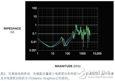
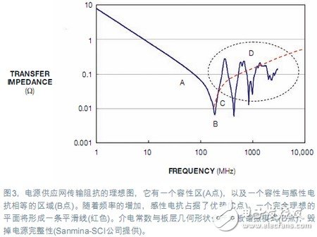
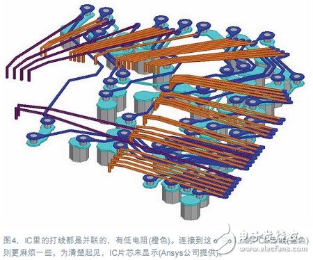
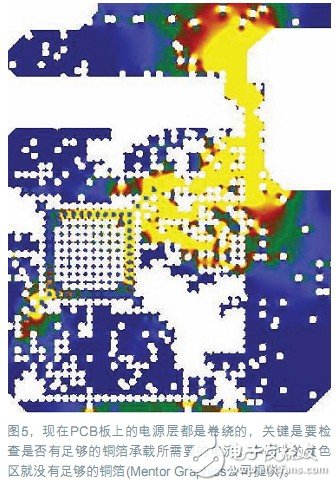
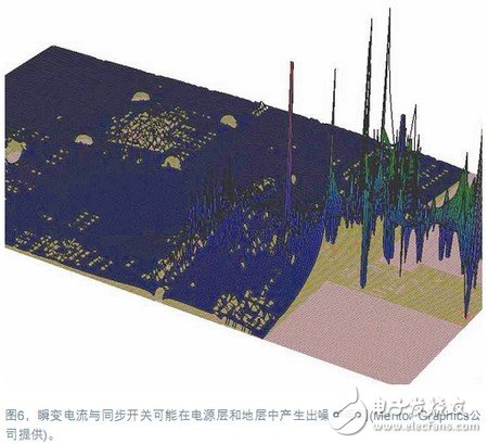
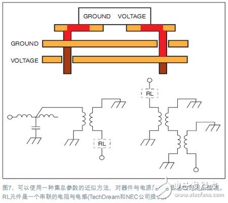
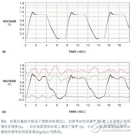
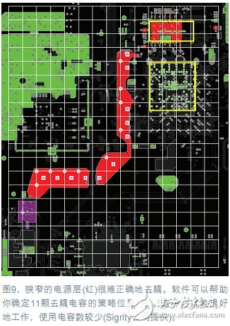
It is no longer a simple task to provide power for chips on a PCB (printed circuit board). In the past, it was sufficient to connect the IC to power and ground through thin traces. These traces did not take up much space. When the chip speed increases, they must be powered by a low-impedance power supply, such as a power layer on the PCB. Sometimes, only one power plane and one ground plane on a four-layer circuit board are needed to solve most power integrity problems. In addition to the power layer, each IC can also be decoupled to solve the cumbersome power problem in the design. However, the current PCB space (and the cost and your schedule) are very tight, and these problems also have an impact on the power supply. Dave Kohlmeier, senior director of simulation and analog series products at Mentor Graphics, said: "Consumer and portable devices are using fewer PCB layers to save costs, but the ICs above them require more voltage levels." These questions Not only affects portable products, industrial products also have space constraints (Figure 1). The circuit of a modern cellular base station is housed in a small box on the antenna, which is usually located in a 19-inch rack inside the building. In high-volume consumer products and automotive products, cost is a key factor. It is definitely unacceptable to put a bunch of capacitors that may not be needed on the PCB. To be successful, the design cycle will be shortened to weeks rather than years. Now, it is impossible to spend time reworking the PCB just to repair and optimize the power and ground planes. Designing power systems for modern electronic products is a daunting challenge. DDR memory works at 1600Mbps and will soon run to 2200Mbps in quad mode. To make matters worse, it is a single-ended output, meaning that your power supply system must cope with the sudden challenge of power supply current. The digital gates in the device may be switching at the same time, and power integrity engineers describe this characteristic as synchronous switching noise. Serial communication has difficult power requirements. The data rate required by the 802.3ba Ethernet standard is 40Gbps and 100Gbps (Reference 1). Modern digital chips operate at voltages below 1V, which means that even millivolt-level noise can cause data-related problems. Multiple chips will increase statistically and cause power supply drop or overvoltage problems. Your system may operate normally for weeks or even months, and the simultaneous switching of all digital circuits at a certain moment causes the system to restart. These power integrity issues are difficult to detect. The power integrity problem of a single chip in the system may affect other chips of the system, resulting in a restart. According to Paul Grohe, an analog application engineer at National Semiconductor, "Even nanosecond power losses can make the system unreliable." Steve Patel, signal integrity product manager at Ansys, said the key to design reliability is to minimize the power supply. Noise means that digital system engineers must understand analog and even RF design concepts. Power system engineers know that the power system must have a low impedance (Figure 2), and the analog engineer's concept is that the noise on the power pins of the analog IC is as small as possible. Unlike digital chips, analog chips have no noise threshold. The PSRR (Power Supply Rejection Ratio) specification specifies how much power supply noise will infiltrate the output pins of the device. Digital system engineers must now cope with the same problem of power supply noise (see sidebar "Please talk to me for another person"). Brad Brim, product marketing manager at Sigrity, said that the power distribution network that supplies power to the chip needs to have a low equivalent inductance: 0.01 nH for the core voltage and 1 nH for the I / O power supply. He pointed out that the power plane will couple noise into the signal. In some cases, a signal line placed between two ground layers has 15mV of noise. When the layout personnel lay the same signal between the power layer and the ground layer, its noise reaches 45mV. Power integrity tools can make a decisive optimization of the design. When you do layout optimization, you cannot use empirical decoupling methods. Ansys ’Patel claims that the software can help you determine the number, type, and cost of capacitors. These tools can also tell you the effect of changing the distance between layers. For example, TechDream President and Founder Yoshi Fukawa said that NEC ’s PI (Power Integrity) Stream can help you by adding or moving capacitors, changing the capacitance and the shape of the layer, and changing the distance between the power layer and the ground layer. Get your own impedance target. Mentor ’s Kohlmeier believes: “You can use CAD files for hypothesis analysis experiments. This is much faster than hardware retry. This is the value of virtual prototypes.†Therefore, the use of simulation software is important so that it can be used in design Make critical decisions early in the phase. Changing the capacitor position, the number of capacitors, and other variables may not affect other departments, but reducing the distance between layers in order to increase the capacitance between layers will affect the entire design team (Figure 3). Sanmina-SCI has a patented modern manufacturing method that can design 4 mil dielectric interlayer thickness, increasing the interlayer capacitance. way of solving the problem Kohlmeier said that power integrity simulation is more difficult than many engineers expected, because each capacitor, connection vias, and power layer structure must be considered. He pointed out that connecting vias at two levels reduces the impedance of the power supply network, so it is as important as capacitance. Unlike power supply integrity, signal integrity generally involves some traces, and signal integrity can be measured in the time domain with an oscilloscope. Using the Z11 impedance curve of Port 1 to Port 1, the simulation of the power supply integrity can obtain the impedance in the frequency domain. To understand the impedance problem of a power layer, a VNA (Vector Network Analyzer) is needed, which is difficult to use. Simulations are complementary to measurements, not replacements. They provide important information about PCB performance before manufacturing. Sigrity's Brim said: "No matter how fast your simulation software is, it can't be faster than a measurement." But he pointed out that you have to have a manufactured PCB to make a quick measurement. You must believe the work done by the IC designer, and believe that the chip used does not have power integrity issues. Ansys ’Patel stated that“ neither the IC nor its bonding wires are the key to power integrity, â€because both IC power pins and bonding wires are connected in parallel (Figure 4). Steve Kaufer, engineering director of HyperLynx at Mentor Graphics, believes that layout engineers who lack technical knowledge to avoid power integrity and signal integrity issues are often the source of the problem. Power integrity software can help you solve DC and AC problems. In addition, the holes between the power layer and the ground layer are RF waveguides. To deal with the DC problem, it must be ensured that the PCB layer can carry the amount of current that needs to be provided. To deal with AC problems, it must be ensured that the power supply system can provide the fast-changing current required by modern chips. Finally, note that the behavior of the waveguide may be non-intuitive. The RF problem is very important in the prevention of EMI (electromagnetic interference) problems. It will prevent your circuit board from passing the FCC (Federal Communications Commission) certification. If the design uses a large board surface, it is important to use simulation, which will produce resonance. If your board will emit RF from the interlayer cavity, using appropriate software simulation can help EMI engineers solve this type of problem. The remedy can be to place capacitors around the edges of the circuit board. Sun Microsystems has a patent of 6727780, which uses a resistor in series with the capacitor so that RF energy can be absorbed at the edge of the circuit board without being reflected back into the structure. Digital chips require large currents, which may cause DC power supply problems (Reference 2). FPGAs and other digital chips require many power supply voltages, so the power supply layer must be split to provide multiple voltage rails. The digital chip also has hundreds of pins, requiring hundreds of vias, which will cover the vast copper foil area of ​​the power and ground layers. It must be ensured that the current density on the copper foil selected for these layers is kept below a reasonable value (Figure 5). High DC current can also cause thermal problems. The temperature coefficient of copper is 0.4% / ° C, which means that for every temperature increase of 25 ° C, the resistance increases by 10%. This increase in resistance occurs under heavy loads, where reliability is critical. The increase in resistance also increases the temperature, reducing the life of components on the circuit board. Once there is enough copper foil to provide DC load, we must pay attention to the AC design of the power layer (Figure 6). Power integrity simulation can check where the return current flows through the power plane. During operation, the current intensity obtained by a digital chip is different and changes in nanoseconds. The power supply system must have a sufficiently low AC impedance that can change with the current (expression is di / dt, that is, current derivative / time derivative), so as not to cause a large change in the power supply voltage of the chip pin. Since di / dt also emits electromagnetic energy, these offsets may cause EMI problems. Therefore, signal integrity, power integrity, and EMI compliance are all interrelated. Without simulation, your design may have crosstalk between vias and other seemingly inexplicable problems. Software selection The actual geometry of a power network is very important to its performance, so most software vendors use field solver technology in their power integrity tools (Reference 3). These tools should give you a quick answer and precise results. RF-IC and system designers generally use full wave field solvers to solve the Maxwell equations in 3D. However, it takes a long time for the 3D field solver to obtain results, especially when used for relatively large physical items, such as PCB boards. Therefore, power integrity vendors have designed hybrid solver technology in their power integrity tools. When solving traces, these tools use a 2D solver that uses the fast technology of transmission line theory. When simulating a plane, the tool can use 2D or 2.5D finite element technology. In some cases, the software can use a lumped parameter component capacitance and inductance model to model vias. To obtain more accurate results, the tool can use a full-wave 3D solver for the vias. In addition, a full-wave solver can also be used to simulate the effects of 3D structures, such as connector pins and other mechanical devices in the power path. Software vendors have also incorporated thermal analysis into their tools. You can use it alone, or output heat information to a dedicated thermal analysis tool, such as Flotor of Mentor Graphics, which is a CFD (Computational Fluid Dynamics) 3D simulation environment. Mentor's HyperLynx simulation tool can do its own thermal analysis and output the results to FloTherm, so that the thermal performance model of the entire system or a chassis can be established. Agilent has redeveloped its own ADS (Advanced Design System) Momentum product, which can provide simulation results for power and ground layers with very many vias. It can also be used for designs where there are few traces in the power layer. MOM (Moment Method) is the fastest simulation method for multi-layer structures. It can solve the full 3D field, including all terms in the Maxwell equation. This full-wave scheme takes into account the high-frequency effects of Faraday's law and the substitution current term that Maxwell adds to the Ampère equation (Reference 4). Using MOM to simulate large-scale layers is very time-consuming, so Agilent has invented some algorithms that can reduce the time required to obtain accurate results. Colin Warwick, the owner of Agilent ’s high-speed digital products, said the tool uses a tree / co-tree approach that can be used all the way to DC. In addition, the lumped parameter analysis method can also be used for planar parts. NEC's PIStreamn software models the plane into a matrix of lumped parameters, making it suitable for analysis using Spice engines and other lumped parameter technologies. For a plane, the software uses PEEC (Partial Element Equivalent Circuit) technology to generate an RLGC (resistance / inductance / conductance / capacitance) equivalent. The software will also establish a lumped parameter model for the via and the cavity formed between the power layer and the ground layer (Figure 7). The software also uses a series RLC (resistance / inductance / capacitance) model to model the decoupling capacitance. This model takes into account the parasitic resistance and capacitance of the capacitor and the parasitic resistance and inductance of the fan-out traces and vias. You can quickly complete the analysis of a single board pair by establishing a simulation run. When changing the settings, the software will do a multi-layer analysis that takes into account all relevant boards. In addition to simulating the physical structure of the finished board, software tools such as HyperLynx can also do early planar planning of circuit board layers and decoupling structures. You can then quickly run an analysis to get some concepts about transmission impedance and other variables. Giga Hertz Technology has developed a faster Spice engine, which is integrated into NEC's PDN (Power Distribution Network) Expert. With these plane planning tools, you can manually outline the PCB and layers to optimize capacitance early in the design. In this way, you can get the concept of board shape, size, stacking, and the number of capacitors. Some power integrity software vendors in the PC world (such as Mentor Graphics and Cadence) have integrated their tools into the design flow. Although this does not eliminate the concern that one supplier provides all the tools, the power integrity simulation uses a physical representation of the PCB to become a geometric model. Both Ansys and Sigrity can accept input from Cadence's Allegro, Mentor Graphics' PADS, and company tools such as Zuken and AlTIum. Agilent's power integrity tools stem from its expertise in RF design. In addition to its use with ADS design tools, the company's EMPro software can also import PCB data from Cadence's Allegro. Customers often use NEC's PIStream together with Zuken's PCB tools, but the software can also accept input data from Cadence's Allegro and other PCB software. Although some engineers prefer integrated tools in their circuit board processes, obtaining tools from simulation specialists such as Ansys has some advantages. For example, the company's SI (Signal Integrity) Wave tool is similar to Mentro Graphics' HyperLynx, and the PIAdvisor tool can help you delve into power integrity issues. The tool has a 3D solver for via simulation. In addition, you can also use Ansys' HFSS (High Frequency Simulator System) tool to do full 3D simulation of physical problems, such as connectors and other 3D geometries. Some customers will output the output of Ansys power integrity tool and signal integrity tool to the same HFSS tool they use to model the chassis. In this way, they can evaluate the EMI of the product. CST (Computer Simulation Technology) EM Studio software can accept Gerber PCB file input and can calculate 3D IR (current / resistance) drop. The software you choose must have the required capabilities. Many companies want you to solve the problem of signal integrity and power integrity separately. They assume that once you fully reduce the power supply impedance, you will pay attention to signal integrity. The problem with this solution is that power supply noise and signal noise interact. To solve this problem, Sigrity allows you to simulate the effect of power supply noise on signal integrity (Figure 8). CST's Microwave Studio can also analyze the noise propagating from the power plane in close proximity. High price problem The price of power integrity software often stuns inexperienced engineers. A simple DC emulator may cost $ 15,000, while a complete system that includes power integrity, signal integrity, and thermal solver may cost $ 75,000. This number seems high for software, but the cost of power integrity failure should be considered. The remanufacturing of a complex circuit board may cost US $ 5,000 or US $ 10,000 in production and engineering, while the cost of not being listed on time is US $ 1 million. Another consideration is the system's BOM (bill of materials) cost. If the power-integrity software can save 50 cents on the capacitor, for a large-volume product, it may be possible to recoup the cost of the power-integrity software in a few months. Antel ’s Patel found that the three engineers who used to do power integrity, signal integrity, and EMI analysis were isolated from each other. Now, although it may still be an engineer doing EMI analysis, this person first has to work with a person who does power integrity and signal integrity analysis. They often share the same software. Sigrity ’s Brim pointed out that IBIS (Input / output buffer specification) 5.0 has power-ground And the signal data allows the simulation software to correlate the noise of the 5.0 model power pin to the noise leaked through the output, similar to the PSRR specification in analog devices. All of these functions combine into one effect, which allows you to have a well-designed and reliable product (Figure 9). If you understand and know how to use these expensive tools, your status as an engineer will double. For engineers who like CAD (computer-aided design) software, learning these tools is not difficult. Mentor Graphics provides HyperLynx free learning courses at many of the company ’s sales locations. If you have experience with other types of emulators, then learning power integrity tools is basically no problem. What needs to be learned and understood is the concept and terminology of the frequency domain, as RF designers do. If you add this knowledge to your existing time domain experience, you can accept the most stringent design challenges and become a winner. French type cable reel Non-rewirable, 230V~, IP20, Class I, with a thermal cut-out, with a non-rewirable plug with cord H05VV-F 3G1,0-1,5mm 2 , French Cable Reel,Electric Cord Reel,Cable Drum,Cable Drum Roller CIXI KYFEN ELECTRONICS CO.,LTD, , https://www.kyfengroup.com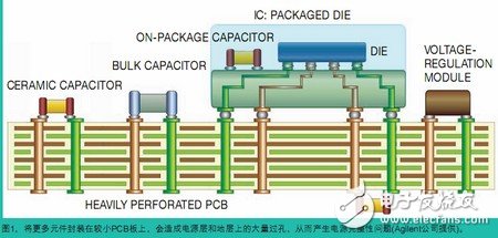

with 4-way socket outlet with or without shutters.