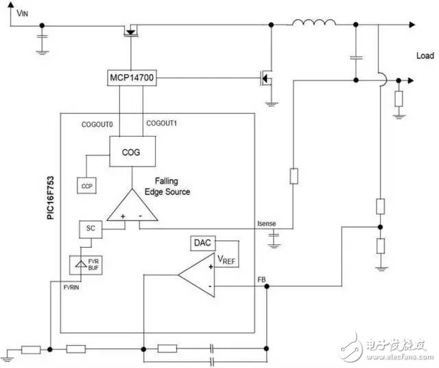
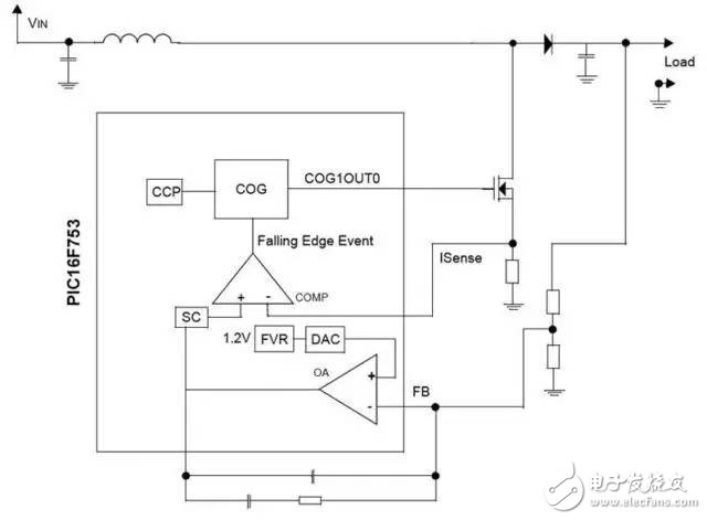
A synchronous analog-controlled synchronous step-down power supply and a step-up power supply can be implemented using the same single-chip microcomputer to achieve output voltage regulation. The two solutions share a common advantage of not taking up any processor resources, so the kernel can fully meet the needs of more complex firmware. At the same time, the analog loop is able to respond more quickly to load steps and input voltage variations, which is very useful for many applications. The microcontroller discussed in this article is Microchip's PIC16F753. The set of peripherals required for a buck or boost converter is identical: complementary output generator, comparator, op amp, 9-bit analog-to-digital converter, fixed reference voltage, slope compensation block, and capture and compare PWM module. These peripherals should be internally connected via firmware to reduce the number of external pins required. Circuit diagram The buck converter has an input voltage range of 8 to 16V DC and an output of 5V DC, 2A and 10W. The code size is 105 words, the RAM capacity is 0 bytes, the available code size is 1943 words, and the available RAM capacity is 128 bytes. The efficiency measured under 2A conditions was 94%. Figure 1: Step-down power supply block diagram Figure 1 shows a block diagram of a synchronous buck power supply. The output voltage here is regulated using peak current mode control and is compared to the reference voltage using an error operational amplifier (OPA). The result is then entered into the peak current comparator. The internal slope compensation module subtracts a software programmable slope from the error amplifier output value and inputs it to the peak current comparator. The CCP Capture and Compare PWM module provides a control signal with a fixed frequency and a fixed duty cycle, while the peak current comparator output is selected as the other (graded) source of the complementary output generator (COG) falling edge. The boost converter has the same working principle, as shown in Figure 2. However, the parameter specifications are slightly different. Specifically, the boost converter has an input voltage range of 3 to 5V DC, while the output and RAM are the same as the buck converter. The code size is 99 words and the available code size is 1949 words. The efficiency measured under the conditions of 2A was 87%. Figure 2: Boost Converter Block Diagram working principle Once the peripherals are configured and connected together, the control loop runs automatically, eliminating the need for processor time. When the duty cycle exceeds 50%, the peak current control scheme requires slope compensation to prevent oscillation. When the duty cycle is low, slope compensation can also help stabilize the control loop if the current sense resistor is small. The PIC16F753 has an internal slope compensation block that can be used to subtract a programmable ramp from the output before feeding the error amplifier output to the peak current comparator. For synchronous switching power supplies, the transistor control signal requires a small dead band to avoid shoot-through current. The COG can generate this signal based on the oscillator frequency or the analog delay chain. With the analog delay chain, the user can set a deadband with a resolution of 5 ns, which is ideal for small transistors. Set the deadband to 30 ns for this particular application. For a buck topology, the inductor current is equal to the load current. In order to be able to measure the peak inductor current using the lower arm current sense resistor, some modifications are required. Normally, the current sense resistor is a filtered output current that cannot be used by the peak current control scheme. When the output capacitor is grounded through a current sense resistor, the ESR increases, but the resulting waveform is very similar to the inductor current waveform. The disadvantage of this method is that the efficiency is slightly lower, but the upper arm current sense resistor usually requires an additional circuit (current mirror or dedicated IC), which increases the cost. In a boost topology, the inductor current is equal to the input current. The inductor peak current is measured directly by the resistor placed between the source of the transistor and ground. Input and output There is no integrated output current limit in the control loop, so the second comparator should be used and selected as the automatic shutdown source for the COG. The error amplifier output is the inductor peak current limit, so keeping this value low through a resistor divider helps avoid inrush current problems and catastrophic short-circuit conditions. However, this method has the disadvantage of a reduction in system gain and a slow response to transients. The OPA output pin is the same as the slope compensation block input pin, so the two peripherals can be used together without any additional external connections. If a resistor divider is used to limit the OPA output voltage, it must be externally connected to the FVR buffer input pin. The input voltage of the boost converter should be connected to the microcontroller via a small diode and bootstrapped to the output. This way, when the output voltage rises, it powers the microcontroller and MOSFET drivers. This achieves an increase in efficiency because a higher VGS will improve RDS(ON), while an interval below 4.5V is a problem for most power transistors. At the same time, this makes the FVR the only existing stable reference voltage, and the circuit also needs to make some changes to ensure that the loop's reference voltage is never affected by the power supply or output voltage. Since the reference voltage of the control loop is derived from the DAC, this peripheral also requires a stable reference. The 1.2V FVR is selected as the DAC reference voltage to meet all of the above requirements. From the power supply through the inductor and rectifier diode to the output, the boost topology has a clear DC current path, even when the switching transistor is blocked. The current limiting circuit only prevents overcurrent before the switching frequency becomes zero. After that, if there is no additional protection switch, a catastrophic short circuit event may occur. Therefore, we can place an extra transistor on the output lower arm to cut off the load when a short circuit occurs. For comparator-based short-circuit protection applications, a stable reference voltage must be ensured over the entire operating voltage range. Since the output current shunt voltage is usually too small to be used directly with the 1.2V FVR, we need to send it externally, first through the FVR buffer, then through the resistor divider to get the reference voltage required by the comparator. . Since the FVR buffer takes this application, the op amp output must be used directly with the slope compensation module instead of an additional voltage divider. This not only does not take up processor time, but also applies more pins and peripherals. For ADC-based short-circuit protection applications, the voltage and FVR values ​​of the current-sense resistor are read in firmware. The FVR voltage needs to be read to calculate the VDD value (below 5V), in this case the ADC reference voltage. Although this does not require the use of additional comparators, I/O pins, or external resistors, it requires some program space and processor time. We must compensate the converter for a specific load and must also verify its stability under all operating conditions. The performance is similar compared to using a dedicated PWM control chip, but the use of PIC microcontrollers increases flexibility. In addition, the analog control loop can operate independently, so the microcontroller core can run the user's algorithm completely, measure various power parameters or send relevant information. application Power supplies that use analog control loops can respond quickly to changes in dynamic loads and input voltages. For current controlled loads such as LEDs or thermoelectric cells, voltage feedback can be replaced by average current feedback. The power supply can also be used in a variety of applications where voltage and current control are required, such as CC and CV battery chargers. The PIC16F753 DAC has 9-bit resolution and can be converted to a minimum voltage step of 20 mV through a 1/2 output voltage divider in a buck converter application and a 1/5 output voltage divider in a boost converter application. Convert to a minimum voltage step of 50 mV. This application requires an op amp, a comparator, and a DAC. The DAC output can be internally connected to an op amp, which saves one pin. The CCP module generates a signal with a fixed frequency and a fixed duty cycle for the COG. Depending on the user option that limits the OPA output, the resistor divider needs to be externally connected to the FVR buffer input. If you do not use a resistor divider, you do not need to use two pins, one is sufficient. In this case, the op amp output pin, which is the same pin as the slope compensation block input pin, is configured as an analog pin and should not be used for other purposes. We can use a digital pin that is only used as an input function as a button or for other similar purposes. During operation, the programming data I/O pins and the other two pins are idle for user-specific purposes. Boost converter alternative design We can also use the PIC12F1501 to create a digitally controlled boost supply. It is highly efficient at light load and hardware overvoltage protection and requires only a small number of components. The required peripherals include two 10-bit ADC channels, an FVR, a comparator, a digitally controlled oscillator, and a complementary waveform generator. The above peripherals are internally connected by firmware, reducing the number of external pins required to three. The block diagram of the application is shown in Figure 3. Figure 3: Digital Control Boost Power Block Diagram We apply a proportional control loop to regulate the output voltage and current. Two ADC channels are used to read the output value and adjust the control signal accordingly. The numerically controlled oscillator uses a variable frequency constant on-time pulse for duty cycle pulse frequency modulation. in conclusion This article shows how to use Microchip microcontrollers to create a buck and boost converter while saving some processing power to perform other tasks. The three application examples in this article only need a small set of peripherals to achieve their respective goals. 1200 Puffs Disposable ecig have a completely enclosed design, reducing the need for charging and replacing cartridges. The no-charge design also reduces the occurrence of faults. It is understood that with rechargeable e-cigarettes, each cartridge needs to be charged at least once and the battery efficiency is extremely low, while the design of disposable ecig can solve this problem very well. 1200 Puff E-Cigarette,1200 Puff E-Cigarette For Sale,Best 1500 Puff E-Cigarette,Best 1200 Puff E-Cigarette For Sale Shenzhen E-wisdom Network Technology Co., Ltd. , https://www.healthy-cigarettes.com