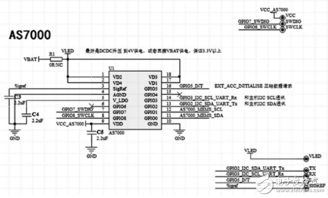
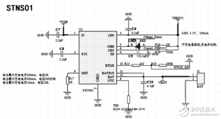
introduction With the development of mobile Internet, technological advancement and the introduction of high-performance low-power processing chips, smart wearable devices are becoming more and more popular, and wearable smart devices have been commercialized from concept to Google Glass, Apple Watch, Samsung Smart Watch, Nike's fuel wristbands, sensor smart suits, solar-powered rechargeable backpacks and other wearable smart devices have emerged, and smart wearable technology has penetrated into many fields such as fitness, medical, entertainment, security, and finance. At present, in the domestic bracelet market, the smart bracelet with high-precision heart rate detection function is becoming more and more mature. Xiaomi has also launched a heart rate bracelet. Its center rate module uses AMS dynamic heart rate detection chip AS7000. 1 System overall plan introduction As shown in Figure 1 based on the AS7000 heart rate wristband system framework, the wristband is mainly composed of the charging management system, the three-axis acceleration sensor LIS3DH step counting motion information system, the AS7000 dynamic heart rate detection system, touch, OLED display, mobile app Bluetooth information. The interactive system is composed of a common system. 1.1 Charging Management System Figure 1 Based on the AS7000 heart rate bracelet system framework The STNS01 integrates an LDO regulator and a battery charge management system. It uses the CC / CV algorithm to charge the battery. The charging current can be selected using an external resistor. The charging current is up to 400mA and the floating voltage is 4.2V. The input supply voltage is typically used to power rechargeable batteries and LDO regulators. When a valid input voltage does not exist and the battery is present, the device automatically switches to battery power. The STNS01 battery charge management system integrates overcharge, overdischarge and overcurrent protection circuits to prevent battery damage under fault conditions. It also has a charge control pin to control the stop charging when we detect the battery overheating from the outside. The STNS0 chip is in shutdown mode and battery power consumption can be reduced to 500 nA, which maximizes battery life, especially during shelf or shipping. The package size of the chip is only 3 & TImes; 3mm, which reduces the space for the PCB layout of the smart bracelet. Figure 2 STNS01 minimum system principle As shown in FIG. 2, the chip 1 pin IN: battery management chip voltage input pin. Chip 2 pin SYS: Battery management chip 3.1V output pin, can provide power, similar to the LDI output pin. Chip 3 pin LDO: Battery management chip 3.1V output pin, see the chip data sheet description. Chip 4 pin SD: LDO output control pin, default pull-up enabled. Chip 5 pin CHG: Battery management chip error prompt pin, flashing indicates that there is a problem with the power supply. Chip 6 pin CEN: Charging enable pin, pull-up enable. Chip 7 pin GND: Ground. Chip 8 pin NTC: External thermistor. Chip 9 pin ISET: charging current control pin, connected to 1kΩ resistor, electric The flow is up to 200mA. Figure 3 Schematic diagram of the minimum system of the three-axis acceleration sensor LIS3DH Chip 10 pin BTMS: Battery voltage output pin, generally used to detect the battery terminal voltage after voltage division. Chip 11 pin BATSNS: Battery positive. Chip 12 pin BAT: Battery positive. 1.2 Triaxial acceleration sensor In the scheme, we used two three-axis accelerometers, one of which is for motion recording. We can use sensors to perform algorithms such as step counting and sleep. Another triaxial accelerometer is used in conjunction with AS7000. Heart rate detection function. Three-axis acceleration We use STMicroelectronics' LIS3DH, which has the lowest operating current consumption of 2uA. This 3&TImes; 3&TImes; 1mm accelerometer is ideal for motion sensing, space and power-constrained applications, especially for smart hands. Application on the ring. As shown in FIG. 3, the chips 4 and 6 are used as I2C communication pins, which are clock lines and data lines for I2C, respectively. The 7th pin of the chip is the slave address selection of the LIS3DH chip. The grounding represents the slave 7-bit address is 0x18, and the 8th pin of the chip is connected to the high level, which means that the I2C communication interface is selected. If the grounding representative selects the SPI communication. interface. Chips 9, 11 pins: respectively correspond to the interrupt signal output pin of the three-axis sensor, generally used for the interrupt signal to the MCU end when the data buffer overflows, which is beneficial for us to manage the power consumption of the MCU when doing the counting algorithm. 1.3 AS7000 Dynamic Heart Rate Detection System Heart rate We use AMS's heart rate detection chip AS7000, which includes highly integrated optical sensors and associated software algorithms. It provides industry-leading high-precision optical heart rate measurement (HRM) and heart rate variability (HRV) measurements. The operation of the AS7000 is based on photoplethysmography (PPG). Changes in the amount of blood flowing through the blood vessels during contraction and expansion of the heart cause expansion and contraction of the blood vessels to modulate the light, and the heart rate can be measured by measuring the modulated light. The heart rate sampling algorithm has been integrated into the AS7000 chip, so we only need to read the data through the I2C interface. As shown in Figure 4, the 13th and 14th pins are I2C communication pins with the Host host. The 7th and 8th pins are the SWD emulation interface of the AS7000, and the AS7000 is an MCU of the M0 core, which is mainly used for the processing of the heart rate algorithm. 8th of which Figure 4 AS7000 principle Pin GPIO8 controls whether the AS7000 chip enters standby mode, GPIO8 outputs high level, AS7000 standby; GPIO8 outputs low level, AS7000 normal operation mode. The 11th and 12th pins are the I2C communication pins of the AS7000 and LIS3DH, mainly because the AS7000 needs to filter out the interference generated during the dynamic heart rate test. The 16th pin is GPIO5. In the dynamic heart rate algorithm, AS7000 requires three-axis accelerometer data. The first one can be used to hang a three-axis accelerometer separately, and the other is to request three axes from the host. Acceleration data. GPIO5 is used in the second way. However, considering the synchronization problem of the three-axis acceleration, we generally recommend the first method. The third pin is the Sigref pin. The AS7000's SWD function can be turned off internally. When we turn off the S WD, we need to connect the Sigref pin to the ground before powering up the A S7000. In the next 5 seconds, the SWD is active, and the program burning function of the AS7000 can be realized through the SWD interface. Pins 1, 2, 17, and 18 are the power supplies for AS7000 LEDs. Our best design is to require a DC/DC boost to 4V. To ensure a large enough LED current, DC/ The DC needs to have an EN enable signal pin to control power consumption. In this scheme, we use the battery voltage directly as the power supply. In the test, we need to pay attention to the test effect of the battery voltage above 3.6V. At the same time, I also used a MOS tube to control the turn-on or turn-off of the entire power supply. 1.4 touch We chose CY's SoC Bluetooth chip CYBL10573, which integrates the CapaciTIve Sigma-Delta (CSD) module to provide first-class signal-to-noise ratio and water resistance. All GPIOs support CapSense, are flexible, and support single-finger and dual-function. Refers to the touch app. 1.5 OLED display Display this block we choose self-illuminating OLED display, as long as there is a set of I2C communication interface can achieve a cool interface display. 1.6 mobile app bluetooth internet In this solution, we use CY's SoC Bluetooth chip CYBL10573, which integrates a low-power BLE Bluetooth module. The BLE subsystem includes a link layer engine and a physical layer. The link layer engine supports both master and slave modes. The link layer engine reduces power consumption by providing time-critical features such as encryption in hardware, with minimal processor intervention and high performance. Key protocol elements such as Host Control Interface (HCI) and link control are implemented in firmware. A Direct Test Mode (DTM) is also provided to enable testing of wireless performance using a standard Bluetooth tester. The physical layer consists of a modem and an RF transceiver that passes through 2.4 at 1 Mbps. The GHz ISM band transmits and receives BLE packets. When transmitting, the module will perform GFSK modulation and convert the digital baseband signal of the packet to a radio frequency before transmitting the BLE packet through the antenna. When receiving, the module performs GFSK demodulation on the RF signal in the antenna to obtain a digital bit stream. The RF transceiver includes an integrated Balun. The Balun provides a single-ended RF port pin that drives an antenna terminal with a 50 ohm resistor through a pi-matching network. The output power can be programmed from –18 dBm to +3 dBm to optimize current consumption for different applications. The final smart bracelet to complete the function: 1. Based on AMS AS7000 dynamic heart rate detection; 2. Based on STMicroelectronics' battery management chip STNS01 power supply and charging power management system; 3. The step-by-step motion detection based on the triaxial acceleration sensor chip LIS3DH; 4, based on CY SoC Bluetooth touch Touch function, and mobile phone App BLE4.0 Bluetooth information interaction function; at the same time to complete SoC Bluetooth's own OTA upgrade and AS7000 heart rate algorithm upgrade function; 5, OLED interface display; Finally, through this program we hope to help customers quickly build their own smart bracelet system. Oem Connector,Audio Connector,Power Supply Connectors,Jack Connector Dongguan Swan Electronic Technology Co., Ltd , https://www.swanconnector.com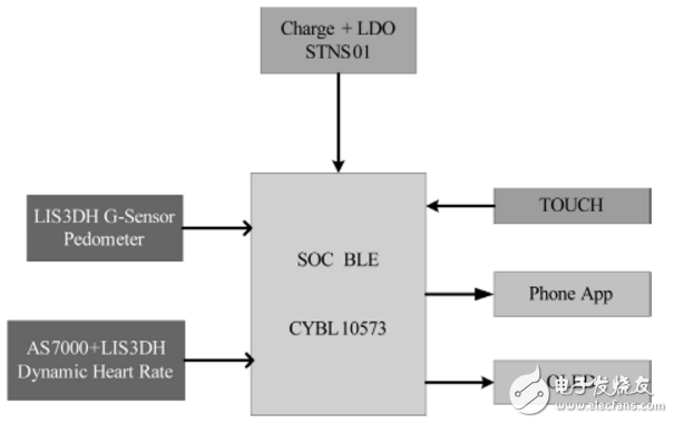
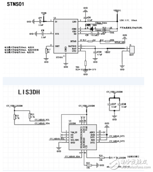
The LIS3DH provides a very accurate test data output over a full range of ±2g/±4g/±8g/±16g, maintaining excellent stability at rated temperature and long hours of operation. In this scenario, we will use LIS3DH to complete the implementation of the step counting function. The pedometer is a daily exercise progress monitor that calculates the number of steps people walk, estimates walking distance, calories burned, and allows people to monitor their fitness intensity, exercise level and metabolism at any time.
Unlike existing optical AFEs that produce raw PPG data, the AS7000 integrated microprocessor runs a special algorithm developed by Amers Semiconductor to convert PPG data into HRM and HRV values. It integrates 2 green LEDs, photosensors, analog front section (AFE), microprocessor M0 and HRM algorithms, which enable high-precision testing, whether we are running, cycling, AS7000 low noise and high sensitivity The analog circuit, combined with an acceleration sensor, filters the false heartbeat PPG signal. At the same time, the application of heart rate monitoring on the smart bracelet should especially consider its power consumption problem. The AS7000 can reduce the power consumption to 579uA in the heart rate continuous test mode, and can reduce it to 0.8uA in the test standby mode.